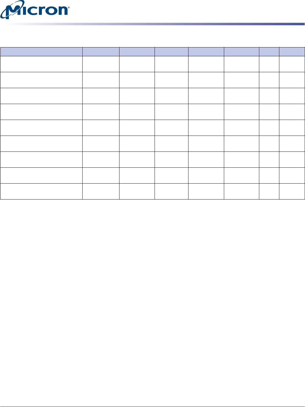
Table 11: x16 I
DD
, I
PP
, and I
DDQ
Current Limits – Rev. E (Continued)
Symbol DDR4-2133
1
DDR4-2400 DDR4-2666 DDR4-2933 DDR4-3200 Unit Notes
I
DD6E
: Self refresh current; 0–
95°C
116 116 116 116 116 mA 11, 22
I
DD6R
: Self refresh current; 0–
45°C
42 42 42 42 42 mA 11, 23,
24
I
DD6A
: Auto self refresh current
(25°C)
17.2 17.2 17.2 17.2 17.2 mA 11, 24
I
DD6A
: Auto self refresh current
(45°C)
42 42 42 42 42 mA 11, 24
I
DD6A
: Auto self refresh current
(75°C)
62 62 62 62 62 mA 11, 24
I
PP6X
: Auto self refresh current
I
PP
current
10 10 10 10 10 mA 11, 24
I
DD7
: Bank interleave read cur-
rent
340 350 360 370 380 mA 4
I
PP7
: Bank interleave read I
PP
current
26 26 26 26 26 mA
I
DD8
: Maximum power-down
current
36 36 36 36 36 mA 11
Notes:
1. DDR4-1600 and DDR4-1866 use the same I
DD
limits as DDR4-2133.
2. When additive latency is enabled for I
DD0
, current changes by approximately +1%.
3. I
PP0
test and limit is applicable for I
DD0
and I
DD1
conditions.
4. The I
DD
values must be derated (increased) when operated outside of the range 0°C ≤ T
C
≤ 85°C:
When T
C
< 0°C: I
DD2P
and I
DD3P
must be derated by +6%; I
DD4R
and I
DD4W
must be derat-
ed by +4%; and I
DD7
must be derated by +11%.
When T
C
> 85°C: I
DD0
, I
DD1
, I
DD2N
, I
DD2NT
, I
DD2Q
, I
DD3N
, I
DD3P
, I
DD4R
, I
DD4W
, and I
DD5R
must
be derated by +3%; I
DD2P
must be derated by +10%.
5. When additive latency is enabled for I
DD1
, current changes by approximately +8%.
6. When additive latency is enabled for I
DD2N
, current changes by approximately +1%.
7. When DLL is disabled for I
DD2N
, current changes by approximately –6%.
8. When CAL is enabled for I
DD2N
, current changes by approximately –30%.
9. When gear-down is enabled for I
DD2N
, current changes by approximately 0%.
10. When CA parity is enabled for I
DD2N
, current changes by approximately +10%.
11. I
PP3N
test and limit is applicable for all I
DD2x
, I
DD3x
, I
DD4x
, I
DD6x
, and I
DD8
conditions; that
is, testing I
PP3N
should satisfy the I
PP
s for the noted I
DD
tests.
12. When additive latency is enabled for I
DD3N
, current changes by approximately +1%.
13. When additive latency is enabled for I
DD4R
, current changes by approximately +4%.
14. When read DBI is enabled for I
DD4R
, current changes by approximately -14%.
15. When additive latency is enabled for I
DD4W
, current changes by approximately +3%.
16. When write DBI is enabled for I
DD4W
, current changes by approximately 0%.
17. When write CRC is enabled for I
DD4W
, current changes by approximately +5%.
18. When CA parity is enabled for I
DD4W
, current changes by approximately +12%.
19. When 2X REF is enabled for I
DD5R
, current changes by approximately –25%.
16Gb: x16 TwinDie Single Rank DDR4 SDRAM
Current Specifications – Limits
CCMTD-1725822587-9947
16gb_x16_1cs_TwinDie.pdf - Rev. G 06/18 EN
19
Micron Technology, Inc. reserves the right to change products or specifications without notice.
© 2015 Micron Technology, Inc. All rights reserved.