LT3582/LT3582-5/LT3582-12
1
3582512fb
TYPICAL APPLICATION
FEATURES
APPLICATIONS
DESCRIPTION
Boost and Single Inductor
Inverting DC/DC Converters with
Optional I
2
C Programing and OTP
The LT
®
3582/LT3582-5/LT3582-12 are dual DC/DC converters
featuring positive and negative outputs and integrated feedback
resistors. The LT3582, with its built-in One Time Programming
(OTP), has confi gurable output settings via the I
2
C interface,
including output voltage settings, power-up sequencing,
power-down discharge, and output voltage ramp rates. LT3582
settings can be changed adaptively in the fi nal product, or set
during manufacturing and made permanent using the built in
non-volatile OTP memory. The positive output voltage can be
set between 3.2V and 12.775V in 25mV steps. The negative
output voltage can be set between –1.2V and –13.95V in
–50mV steps. The LT3582-5 and LT3582-12 are pre-confi gured
at the factory for ±5V and ±12V outputs respectively, and as
such, don’t require the use of the I
2
C interface.
The LT3582 series includes two monolithic converters,
one Boost and one Inverting. The Boost converter has an
integrated power switch and output disconnect switch.
The Inverting converter uses a single inductor topology
and includes an integrated power switch. Both Boost
and Inverting converters use a novel** control scheme
resulting in low output voltage ripple while allowing for high
conversion effi ciency over a wide load current range. The
LT3582 series is available in a 16-pin 3mm × 3mm QFN.
±12V Supplies from a Single 5V Input
n
Output Voltages:
3.2V to 12.775V and –1.2V to –13.95V (LT3582)
5V and –5V (LT3582-5)
12V and –12V (LT3582-12)
n
Digitally Re-Programmable (LT3582) via I
2
C for:
Output Voltages
Power Sequencing
Output Voltage Ramp Rates
n
Power-Up Defaults Settable with Non-Volatile OTP
(LT3582)
n
I
2
C Compatible Interface (Standard Mode*)
n
All Power Switches Integrated
350mA Current Limit (Boost)
600mA Current Limit (Inverting)
n
All Feedback Resistors Integrated
n
Input Voltage Range: 2.55V to 5.5V
n
Low Quiescent Current
325A in Active Mode
0.01A in Shutdown Mode
n
Integrated Output Disconnect
n
Tiny 16-Pin 3mm × 3mm QFN Package
n
AMOLED Power
n
CCD Power
n
General Purpose DC/DC Conversion
L, LT, LTC, LTM, Linear Technology and the Linear logo are registered trademarks of Linear
Technology Corporation. All other trademarks are the property of their respective owners.
* Input thresholds are reduced to allow communication with low voltage digital ICs.
(See Electrical Characteristics).
** Patent Pending
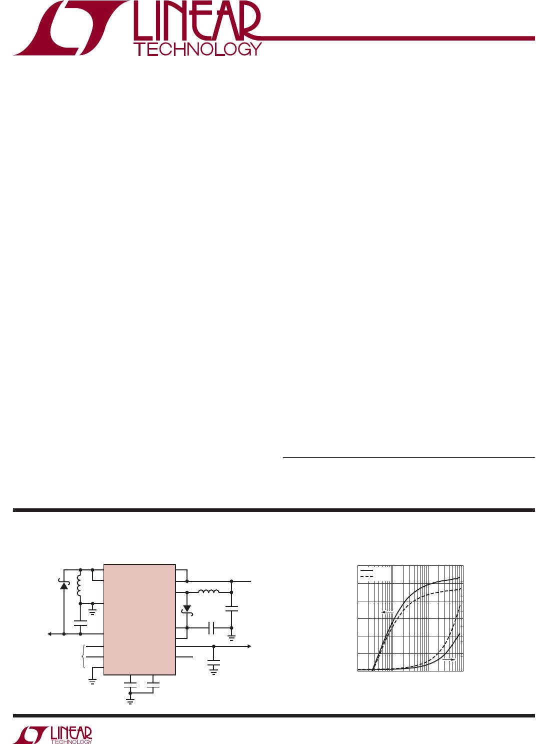
Effi ciency and Power Loss
LT3582
V
IN
SWP
CAPP
V
NEG
–12V
85mA
CAPP
V
PP
SDA
SCL
CA
GND
SWN
SWN
V
OUTN
V
OUTP
SHDN
INPUT
4.5V TO 5.5V
V
POS
12V
80mA
6.8µH
10µF
10nF10nF
RAMPNRAMPP
4.7µF
4.7µF
1µF
6.8µH
3582512 TA01a
I
2
C
INTERFACE
OPTIONAL ON
LT3582-5/LT3582-12

LOAD CURRENT (mA)
0.1
35
EFFICIENCY (%)
POWER LOSS (mW)
45
350
300
250
200
150
100
50
0
55
65
75
85
95
1 10 100
3582512 TA01b
V
OUTP
V
OUTN
LT3582/LT3582-5/LT3582-12
2
3582512fb
PIN CONFIGURATION ABSOLUTE MAXIMUM RATINGS
V
IN
Voltage ..................................................................6V
SWP Voltage .............................................................15V
SWN Voltage ........................................................ 16.5V
CAPP Voltage ............................................................15V
CAPP-V
OUTP
Voltage .................................... 0.8V to 8V
I
CAPP-VOUTP
....................................................... ±300mA
V
OUTP
Voltage ...........................................................15V
V
OUTN
Voltage ...................................................... 16.5V
RAMPP Voltage ..........................................................3V
RAMPN Voltage ..........................................................3V
SHDN Voltage ................................................ –0.5 to 6V
V
PP
Voltage ...................................................0.2 to 16V
SDA, CA, SCL Voltage .................................... –0.5 to 6V
Operating Junction Temperature Range (Notes 3, 5)
LT3582E ............................................ 40°C to 125°C
Storage Temperature Range .............. 65°C to 150°C
(Note 1)
16 15 14 13
5 6 7 8
TOP VIEW
17
GND
UD PACKAGE
16-PIN (3mm × 3mm) PLASTIC QFN
9
10
11
12
4
3
2
1CA
V
OUTN
SWN
SWN
SWP
CAPP
CAPP
V
OUTP
SCL
SDA
V
PP
GND
V
IN
RAMPN
RAMPP
SHDN
T
JMAX
= 125°C, θ
JA
= 68°C/W
EXPOSED PAD (PIN #17) IS GND, MUST BE SOLDERED TO PCB
SYMBOL PARAMETER CONDITIONS MIN TYP MAX UNITS
V
IN_MIN
Minimum Operating Voltage
l
2.4 2.475 2.55 V
V
IN_MAX
Maximum Operating Voltage
l
5.5 V
I
VIN
V
IN
Quiescent Current Ramp Current Confi gured to 1A,
SWOFF Bit Active
325 450 µA
I
VIN_SHDN
V
IN
Quiescent Current in Shutdown V
SHDN
= 0 0.01 0.5 µA
I
CAPP_SHDN
CAPP Quiescent Current in Shutdown V
SHDN
= 0, V
CAPP
= 5.0V, V
OUTP
= 0V 0 0.5 µA
T
OFF_MINP
Minimum Switch Off Time Boost Switch 100 ns
T
OFF_MINN
Minimum Switch Off Time Inverting Switch 125 ns
ORDER INFORMATION
LEAD FREE FINISH TAPE AND REEL PART MARKING PACKAGE DESCRIPTION TEMPERATURE RANGE
LT3582EUD#PBF LT3582EUD#TRPBF LDDB
16-Pin (3mm × 3mm) Plastic QFN
–40°C to 125°C
LT3582EUD-5#PBF LT3582EUD-5#TRPBF LDVG
16-Pin (3mm × 3mm) Plastic QFN
–40°C to 125°C
LT3582EUD-12#PBF LT3582EUD-12#TRPBF LDVH
16-Pin (3mm × 3mm) Plastic QFN
–40°C to 125°C
Consult LTC Marketing for parts specifi ed with wider operating temperature ranges.
Consult LTC Marketing for information on non-standard lead based fi nish parts.
For more information on lead free part marking, go to: http://www.linear.com/leadfree/
For more information on tape and reel specifi
cations, go to: http://www.linear.com/tapeandreel/
ELECTRICAL CHARACTERISTICS
The l denotes the specifi cations which apply over the full operating
temperature range, otherwise specifi cations are at T
A
= 25°C. V
IN
= 3.6V, V
SHDN
= V
IN
unless otherwise noted. (Note 3)
Switching Regulator Characteristics
LT3582/LT3582-5/LT3582-12
3
3582512fb
ELECTRICAL CHARACTERISTICS
The l denotes the specifi cations which apply over the full operating
temperature range, otherwise specifi cations are at T
A
= 25°C. V
IN
= 3.6V, V
SHDN
= V
IN
unless otherwise noted. (Note 3)
Switching Regulator Characteristics
SYMBOL PARAMETER CONDITIONS MIN TYP MAX UNITS
T
ON_MAX
Maximum Switch On-Time Inverting and Boost Switches 10 µs
I
LIMIT_P
Boost Switch Current Limit
l
285 350 430 mA
I
LIMIT_N
Inverting Switch Current Limit
l
490 600 720 mA
R
ON_P
Boost Switch On-Resistance I
SWP
= 200mA 500 mΩ
R
ON_N
Inverting Switch On-Resistance I
SWN
= –400mA 560 mΩ
I
OFF_P
Boost Switch Leakage Current into
SWP Pin
V
SWP
= 5V 0.01 0.5 µA
I
OFF_N
Inverting Switch Leakage Current Out of
SWN Pin
V
IN
= 5.0, V
SWN
= 0.0 0.01 1 µA
R
ON_DIS
Output Disconnect Switch
On-Resistance
V
CAPP
= 10V, RAMPP > 1.4V 1.4
I
LIMIT_DIS
Output Disconnect Current Limit
l
124 155 186 mA
I
VOUTP_PDS
V
OUTP
Power-Down Discharge Current V
OUTP
= 8V 2.4 4.8 8.8 mA
I
CAPP_PDS
CAPP Power-Down Discharge Current CAPP = 8V 1.2 2.4 4.4 mA
I
VOUTN_PDS
V
OUTN
Power-Down Discharge Current V
OUTN
= –8V –1.4 –2.8 –4.2 mA
T
START-UP
Confi guration Start-Up Delay V
IN
> V
IN_MIN
and SHDN > V
SHDN_VIH
to I
2
C
Enabled and Power-Up Sequencing Start
l
64 128 s
Programmable Output Characteristics (Note 6)
SYMBOL PARAMETER CONDITIONS MIN TYP MAX UNITS
V
VOUTP
Positive Output Voltage LT3582-5
LT3582-12
l
l
4.95
11.88
5
12
5.05
12.1
V
V
N_V
OUTP
Positive V
OUTP
Resolution (Note 2) 9 Bits
V
VOUTP_LSB
V
OUTP
LSB (Note 2) 25 mV
V
VOUTP_FS
V
OUTP
Full-Scale Voltage (Note 2) Code = BFh, V
PLUS
= 1
l
12.56 12.775 12.94 V
V
VOUTP_MIN
V
OUTP
Minimum Voltage (Note 2) Code = 00h, V
PLUS
= 0
l
3.152 3.20 3.248 V
V
VOUTP_LR
V
OUTP
Line Regulation Code = BFh, 2.575 < V
IN
< 5.5 –0.02 %/V
V
VOUTN
Negative Output Voltage LT3582-5
LT3582-12
l
l
–5.075
–12.1
–5
–12
–4.925
–11.868
V
V
N_V
OUTN
Negative V
OUTN
Resolution (Note 2) 8 Bits
V
VOUTN_LSB
V
OUTN
LSB (Note 2) –50 mV
V
VOUTN_FS
V
OUTN
Full-Scale Voltage (Note 2) Code = FFh
l
–14.2 –13.95 –13.7 V
V
VOUTN_MIN
V
OUTN
Minimum Voltage (Note 2) Code = 00h
l
–1.23 –1.205 –1.18 V
V
VOUTN_LR
V
OUTN
Line Regulation Code = FFh, 2.575 < V
IN
< 5.5 –0.01 %/V
INL_V
OUTP
V
OUTP
Integral Nonlinearity (Notes 2, 4)
l
±0.6 LSB
DNL_V
OUTP
V
OUTP
Differential Nonlinearity (Notes 2, 4)
l
±0.6 LSB
INL_V
OUTN
V
OUTN
Integral Nonlinearity (Note 2)
l
±0.85 LSB
DNL_V
OUTN
V
OUTN
Differential Nonlinearity (Note 2)
l
±0.85 LSB
I
RAMP00
RAMPP/RAMPN Pull-Up Current
IRMP Code = 00
V
RAMPP
= 0.0V
V
RAMPN
= 0.0V
l
0.7 1.0 1.3 µA
I
RAMP01
RAMPP/RAMPN Pull-Up Current (Note 2)
IRMP Code = 01
V
RAMPP
= 0.0V
V
RAMPN
= 0.0V
l
1.4 2.0 2.6 µA

LT3582EUD-5#TRPBF

Mfr. #:
Manufacturer:
Analog Devices / Linear Technology
Description:
Switching Voltage Regulators Programmable Boost and Single Inductor Inverting DC/DC Converters with OTP
Lifecycle:
New from this manufacturer.
Delivery:
DHL FedEx Ups TNT EMS
Payment:
T/T Paypal Visa MoneyGram Western Union