LT3582/LT3582-5/LT3582-12
13
3582512fb
CMDR: The Command Register is used to control various
functions of the chip. During shutdown and power-up the
CMDR is initialized to 00h.
The RSEL (Register Select) bits are functional only for
the LT3582. The LT3582-5 and LT3582-12 function as if
the RSEL bits are always “0”. These bits perform three
functions:
Each RSEL bit instructs the chip whether to use the
confi guration data from the corresponding OTP byte
(RSELx = 0) or the REG byte (RSELx = 1). Changing an
RSELx bit immediately updates the chip confi guration.
Each RSEL bit determines if I
2
C reads return data from
the corresponding OTP byte (RSELx = 0) or the REG
byte (RSELx = 1).
OTP programming only programs data to the bytes with
corresponding RSEL bits set high.
Setting the SWOFF bit immediately disables the Boost
and Inverting power switches and opens the output dis-
connect PMOS switch. It is recommended to set this bit
before writing new confi guration data. This can prevent
unexpected chip behavior while modifying the confi gura-
tion and also forces a soft-start after SWOFF is cleared
(see
Soft-Start and Power-Up Sequencing
). Writing “1”
to the RST bit resets the internal I
2
C logic and the CMDR
register. Reading bit 6 of the CMDR returns the FAULT bit
indicating if an OTP programming attempt may have failed.
FAULT is cleared during reset, power-up, or by writing a “1”
to the CF (Clear Fault) bit. Conditions that set the FAULT
bit are (1) OTP programming in which the V
PP
voltage
is too low or (2) attempted OTP programming when the
LOCK bit is set.
OTP write attempts that set the FAULT bit
due to low V
PP
voltage should be considered failures and
the device should be discarded. Attempts to re-program
the OTP memory after the FAULT bit has been set are not
recommended.
Finally, setting the WOTP bit starts the
OTP programming.
Table 1: LT3582 Series Register Map
REGISTER
ADDRESS
REGIS-
TER
NAME
BIT BIT
NAME
DESCRIPTION
00h REG0/
OTP0
7:0 V
P
V
OUTP
Output Voltage (00h=3.2V,
BFh = 12.75V)
01h REG1/
OTP1
7:0 V
N
V
OUTN
Output Voltage (00h=1.2V,
FFh = 13.95V)
7 - Reserved, Write to 0
6 LOCK Lockout Bit: See the
OTP
Programming Lockout
Section.
02h
REG2/
OTP2
5V
PLUS
V
OUTP
Output Voltage Bit: Increase
V
OUTP
by ~25mV
4:3 IRMP RAMPP and RAMPN Pull-Up
Current: I
RAMP
= (2)
IRMP
µA
2 PDDIS Power-Down Discharge Enable.
PUSEQ Must be 11 if Set.
1:0 PUSEQ Power-Up Sequencing: 00 =
Outputs Disabled, 01 = V
OUTN
Ramp 1st, 10 = V
OUTP
Ramp 1st,
11 = Both Ramp Together
7 WOTP Write OTP Memory
6 CF/
FAULT
Clear Fault/OTP Programming
Fault
5 RST Reset
4 SWOFF Switches-Off
04h CMDR 3 - Reserved, Write to 0
2 RSEL2 Register Select 2 (0 = OTP2,
1 = REG2)
1 RSEL1 Register Select 1 (0 = OTP1,
1 = REG1)
0 RSEL0 Register Select 0 (0 = OTP0,
1 = REG0)
OTP0/REG0 and OTP1/REG1: Data in addresses 00h and
01h is used to set the output voltages of the Boost and
Inverting converters respectively. See
Setting the Output
Voltages
for more information.
APPLICATIONS INFORMATION
LT3582/LT3582-5/LT3582-12
14
3582512fb
OTP2/REG2: Data in address 02h confi gures the output
voltage sequencing, sets a fi ne voltage adjust for V
OUTP
,
and determines if further OTP programming is permitted or
not. Proper uses of the bits in address 02h are discussed
in the following sections.
Setting the Output Voltages (V
P
, V
PLUS
and V
N
Bits)
The LT3582 series contains two resistor dividers which are
programmable in the LT3582, to set the output voltages.
The positive output voltage V
OUTP
is adjustable in 25mV
steps by setting the V
P
bits in REG0/OTP0 in addition to
the V
PLUS
bit in REG2/OTP2.
V
OUTP
= 3.2V + (V
P
• 50mV) + (V
PLUS
• 25mV)
where:
V
P
= an integer value from 0 to 191
V
PLUS
= 0 or 1
The V
OUTN
voltage is adjustable in –50mV steps by setting
the V
N
bits in REG1/OTP1.
V
OUTN
= –1.2V – (V
N
• 50mV)
where:
V
N
= an integer value from 0 to 255
Dynamically Changing the Output Voltage (LT3582 Only):
After output regulation has been reached, it’s possible to
change the output voltages by writing new values to the
V
N
or V
P
bits. When reducing the magnitude of an out-
put voltage, it will decay at a rate dependent on the load
current and capacitance. Confi guring a large increase in
magnitude of an output voltage can cause a large increase
in switch current to charge the output capacitor. Before
reconfi guring the outputs, consider forcing a soft-start
by asserting the SWOFF bit before writing the new V
P
or
V
N
codes. Subsequently clearing SWOFF initiates the new
soft-start sequence.
Soft-Start/Output Voltage Ramping (IRMP Bits)
The LT3582 series contains soft-start circuitry to control the
output voltage ramp rates, therefore limiting peak switch
currents during start-up. High switch currents are inherent
in switching regulators during start-up since the feedback
loop is saturated due to V
OUT
being far from its fi nal value.
The regulator tries to charge the output capacitor as quickly
as possible which results in large currents.
Capacitors must be connected from RAMPP and RAMPN
to ground for soft-start. During shutdown or when the
SWOFF bit is set, the RAMP capacitors are discharged
to ground. After SHDN rises or SWOFF is cleared, the
capacitors are charged by programmable (LT3582 only)
currents, thus creating linear voltage ramps. The V
OUT
voltages ramp in proportion to their respective RAMP
voltages according to:
V
OUT
_RAMP _RATE =
V
OUT
0.8V
I
RAMP
C
RAMP
Volts / Sec
Proportionality Constant
RAMP pin ramp rate (V/Sec)
where:
I
RAMP
= RAMP pin charging current set by IRMP
bits (1A, 2A, 4A or 8A for LT3582,
1µA for LT3582-5/LT3582-12)
C
RAMP
= External RAMP pin capacitor (Farads)
V
OUT
= Output voltage during regulation
For example, selecting I
RAMP
= 1A, C
RAMP
= 10nF and
V
OUTP
= 12V results in a power-up ramp rate of 1.5Volt/ms
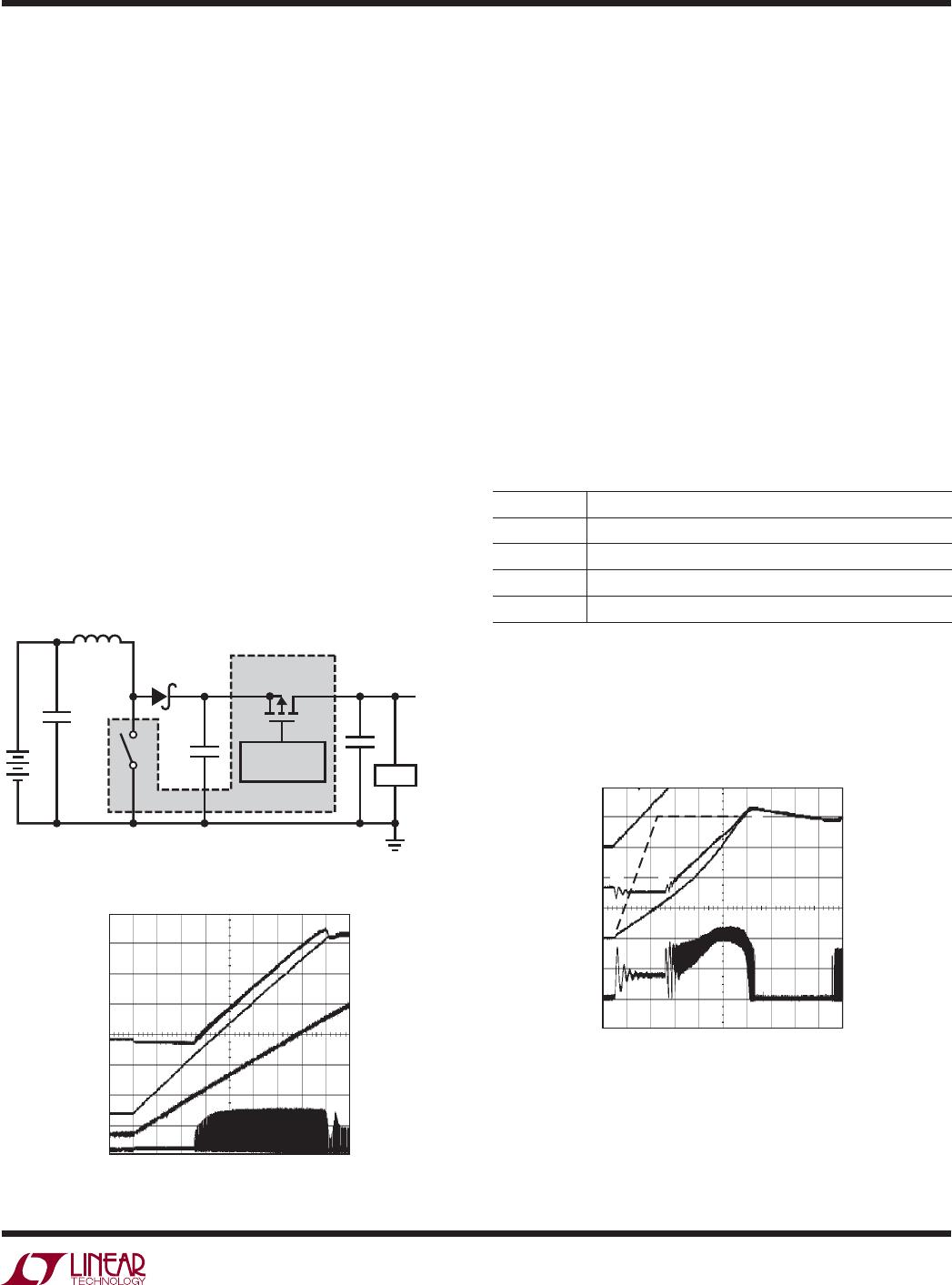
(see Figure 6).
Ramp rates less than 1-10V/ms generally result in good
start-up characteristics. The outputs should linearly follow
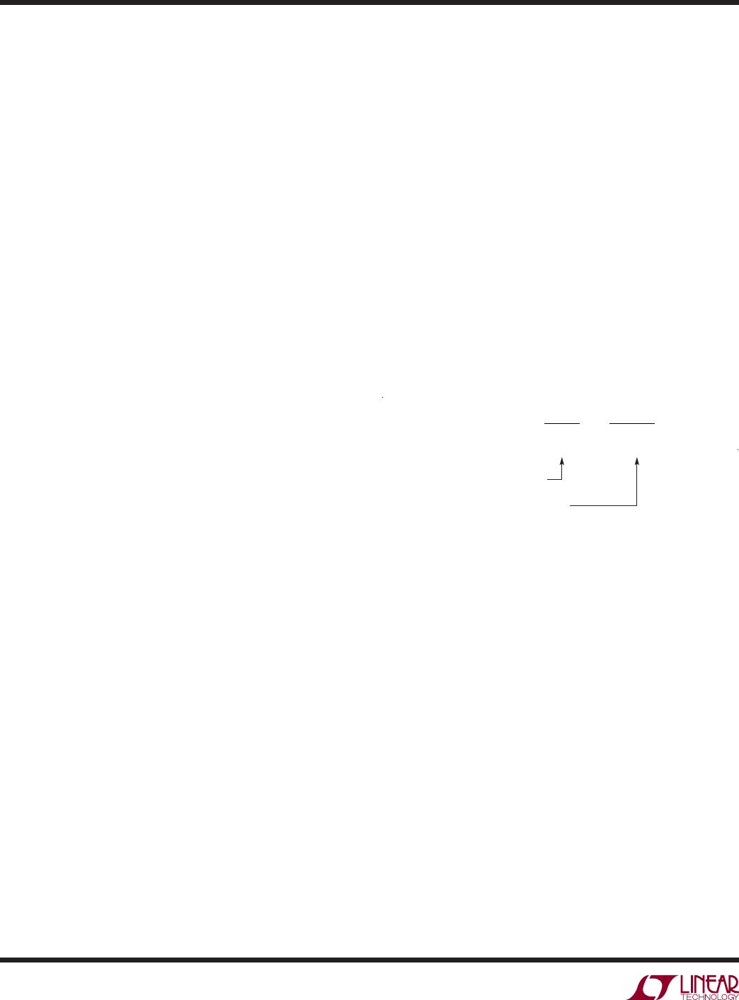
the RAMPx voltages with no distortions. Figure 7 shows
an excessive start-up ramp rate of ~120V/ms in which
APPLICATIONS INFORMATION
LT3582/LT3582-5/LT3582-12
15
3582512fb
several start-up issues have occurred: A) the expected
V
OUTP
ramp up path is not followed B) inductor current
ringing occurs C) the V
OUTP
ramp rate is limited due to
the output disconnect current limit being reached D) ad-
ditional ringing occurs when the CAPP pin starts charging
E) output voltage overshoot occurs because the inductor
currents are maximized during the output ramp-up.
In some cases it may be desirable to use only one RAMP
pin capacitor. In cases where PUSEQ = 11 (see the
Power-
Up Sequencing
section) the RAMPP and RAMPN pins
can be connected together and to a single capacitor. In
this case the capacitor will charge with twice the current
confi gured by the IRMP bits.
Ramping V
OUTP
from Ground: The LT3582 series has
the unique ability to generate a smooth V
OUTP
voltage
ramp starting from ground and continuing all the way up
to regulation (see Figure 6). This ability is not possible
with typical Boost converters in which the output is taken
from the cathode of the Schottky diode (CAPP node in
Figure 5).
L1
D1
SWP
C1
V
OUTP
C3
V
IN
C2
CAPP
LT3582
SERIES
DISCONNECT
CONTROL
LOAD
3582512 F05
APPLICATIONS INFORMATION
The LT3582 series incorporates an output disconnect
PMOS allowing V
OUTP
to be grounded during shutdown.
Once enabled, the Disconnect Control circuit actively
drives the PMOS gate allowing V
OUTP
to ramp up linearly
as shown in Figure 6. Once V
OUTP
reaches regulation,
the PMOS is fully turned “on” to reduce resistance and
improve effi ciency.
Power-Up Sequencing (PUSEQ bits)
Once enabled, the part requires a delay of T
START-UP
(64s
typ) to properly confi gure itself. Once confi gured, the order
in which V
OUTP
and V
OUTN
ramp to regulation is controlled
by the PUSEQ bits. The combinations available for the
LT3582 are shown in Table 2. The LT3582-5/LT3582-12
are pre-confi gured with the 11 combination.
Table 2. Power-Up Sequences
PUSEQ[1:0] Power-Up Sequence
00 Outputs are disabled, neither output ramps up
01 V
OUTN
ramps up 1st, followed by V
OUTP
10 V
OUTP
ramps up 1st, followed by V
OUTN
11 Both V
OUTP
and V
OUTN
ramp-up starting at the same time.
Selecting the 01 or 10 combinations cause one of the out-
puts to start ramping shortly after SHDN rises. The ramp
rate of V
OUT
is controlled by the RAMP pin as discussed
in the Soft-Start section. After V
OUT
nears its target regula-
Figure 5. Boost Converter Topology
Figure 6. V
OUTP
Soft-Start Ramping from Ground
Figure 7. V
OUTP
Soft-Start with Excessive Ramp Rate
3582512 F06
CAPP
2V/DIV
I
L2
0.2A/DIV
V
RAMPP
0.2V/DIV
V
OUTP
2V/DIV
1ms/DIV
3582512 F07
V
OUTP
3V/DIV
V
RAMPP
0.5V/DIV
CAPP
3V/DIV
I
L2
0.2A/DIV
50μs/DIV
A
C
E
BD

LT3582EUD-5#TRPBF

Mfr. #:
Manufacturer:
Analog Devices / Linear Technology
Description:
Switching Voltage Regulators Programmable Boost and Single Inductor Inverting DC/DC Converters with OTP
Lifecycle:
New from this manufacturer.
Delivery:
DHL FedEx Ups TNT EMS
Payment:
T/T Paypal Visa MoneyGram Western Union