LT3582/LT3582-5/LT3582-12
19
3582512fb
Maximum Load Currents: Use one of the following equa-
tions to estimate the maximum output load current for the
positive and negative output voltages:
I
OUTP
=
V
IN(MIN)
V
OUTP
⎛
⎝
⎜
⎞
⎠
⎟
• I
PK
–
T
OFF _MIN
•(V
OUTP
+ 0.5 – V
IN(MIN)
)
2•L
⎛
⎝
⎜
⎞
⎠
⎟
•0.8η
or I
OUTN
=
V
IN(MIN)
V
IN(MIN)
+|V
OUTN
|
⎛
⎝
⎜
⎜
⎞
⎠
⎟
⎟
• I
PK
–
T
OFF _MIN
•(|V
OUTN
| +0.5)
2•L
⎛
⎝
⎜
⎞
⎠
⎟
•0.8η
where:
V
OUT
= Regulation voltage
V
IN(MIN)
= Minimum input voltage.
I
PK
= Peak inductor current. See the
Peak
Current Rating
section. Use minimum
I
LIMIT
rating for these calculations.
η = Power conversion effi ciency (about 88%
for Boost or 78% for Inverting)
T
OFF_MIN
= Minimum switch off time. Typically 100ns
for Boost and 125ns for Inverting.
I
OUT
= Output load current
For example, if V
OUTP
= 10V, V
OUTN
= –10V, V
IN
= 5V, and
L = 4.7H then I
OUTP
= 117mA and I
OUTN
= 105mA.
Note: The 155mA (Typ) current limit of the output dis-
connect PMOS (see Electrical Characteristics) may limit
maximum I
OUTP
unless CAPP is shorted to V
OUTP
. See the
Improving Boost Converter Effi ciency
section.
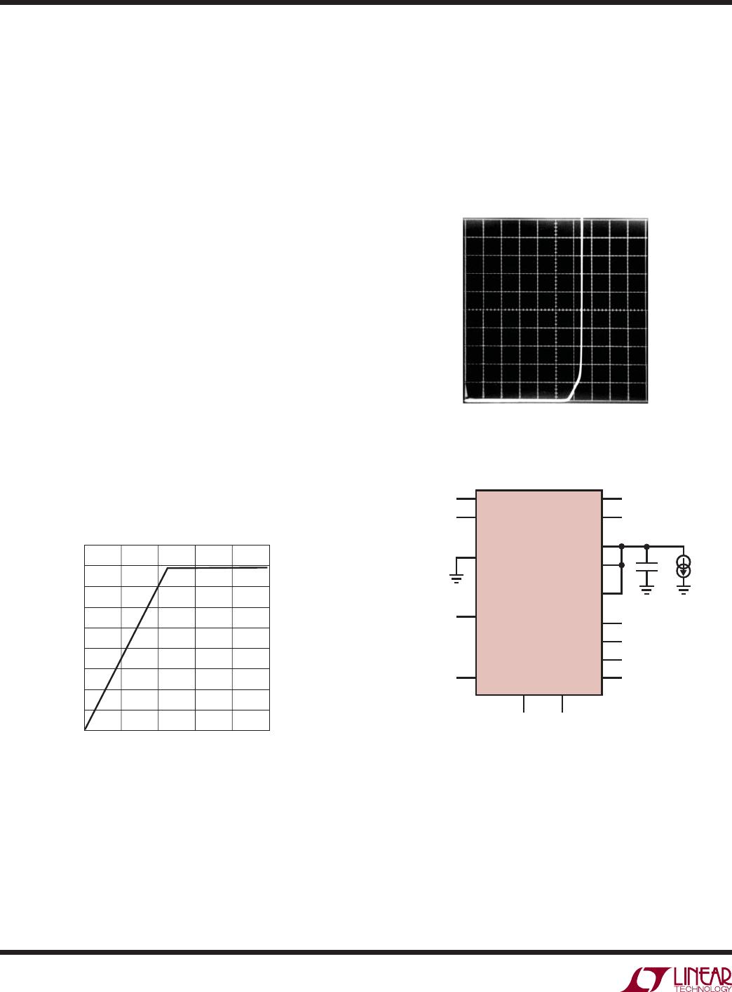
Maximum Slew Rate: Lower inductance causes higher
current slew rates which can lead to current limit over-
shoot. Choose an inductance higher than L
MIN
to limit
the overshoot:
L
MIN
= V
IN(MAX)
• 0.2µH
where V
IN(MAX)
is the maximum input voltage. Using the
previous example V
IN
= 3V, L
MIN
= 0.6H.
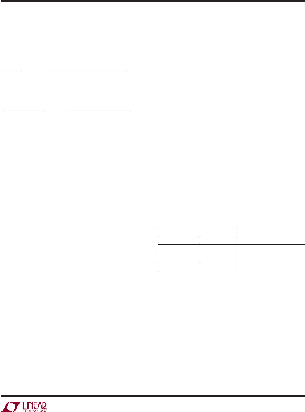
Capacitor Selection
The small size and low ESR of ceramic capacitors makes
them suitable for most LT3582 series applications. X5R
and X7R types are recommended because they retain their
capacitance over wider voltage and temperature ranges
than other types such as Y5V or Z5U. A 4.7F input capaci-
tor and a 2.2F to 10F output capacitor are suffi cient for
most LT3582 series applications. Always use a capacitor
with a suffi cient voltage rating. Many capacitors rated at
2.2F to 10F, particularly 0805 or 0603 case sizes, have
greatly reduced capacitance at the desired output voltage.
Generally a 1206 capacitor will be adequate. A 0.22F to
1F capacitor placed on the CAPP node is recommended
to fi lter the inductor current while the larger 2.2F to 10F
placed on the V
OUTP
and V
OUTN
nodes will give excellent
transient response and stability. Avoid placing large value
capacitors (generally > 6.8F) on both CAPP and V
OUTP
.
This confi guration can be less stable since it creates two
poles, one at the CAPP pin and the other at the V
OUTP
pin, which can be near each other in frequency. Table 4
shows a list of several capacitor manufacturers. Consult
the manufacturers for more detailed information and for
their entire selection of related parts.
Table 4. Ceramic Capacitor Manufacturers
MANUFACTURER PHONE URL
Kemet 408-986-0424 www.kemet.com
Murata 814-237-1431 www.murata.com
Taiyo Yuden 408-573-4150 www.t-yuden.com
TDK 847-803-6100 www.tdk.com
Diode Selection
Schottky diodes, with their low forward voltage drops and
fast switching speeds, are recommended for use with the
LT3582 series. The Diodes Inc. B0540WS is a very good
choice in a small SOD-323 package. This diode is rated to
handle an average forward current of 500mA and performs
well across a wide temperature range. Schottky diodes
with very low forward voltage drops are also available.
These diodes may improve effi ciency at moderate and cold
temperatures, but will likely reduce effi ciency at higher
temperatures due to excessive reverse leakage currents.
APPLICATIONS INFORMATION