LT3582/LT3582-5/LT3582-12
16
3582512fb
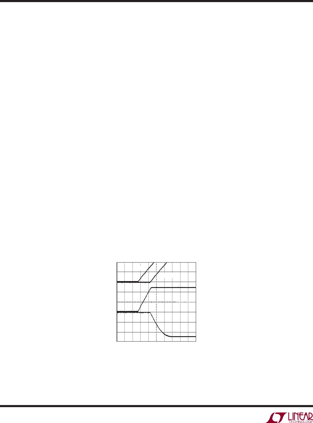
tion voltage, the remaining output is activated and ramps
under control of its respective RAMP pin (see Figure 8).
The power-up sequencing concludes when both outputs
have reached regulation.
Evaluating PUSEQ Settings (LT3582 Only): After SHDN
rises, the LT3582 uses the PUSEQ confi guration found
in OTP. The effects of differing PUSEQ settings can be
observed without writing to OTP by taking the following
actions:
1. Write the SWOFF bit high, stopping both converters
and discharging the RAMP pins.
2. Write the desired settings to the PUSEQ bits in REG2.
3. Set the RSEL2 bit high which selects the REG2 con-
guration settings.
4. Write SWOFF low which restarts both converters.
This will initiate the desired power-up sequence that can
be observed with an oscilloscope.
Power-Down Discharge (PDDIS bit)
The PDDIS bit is used to enable power-down discharge.
This bit is pre-confi gured to a “1” for the LT3582-5 and
LT3582-12, thus enabling power-down discharge.Setting
PDDIS = 0 disables the power-down discharge causing
the chip to shut down immediately after SHDN falls.
APPLICATIONS INFORMATION
The PDDIS bit must only be set in conjunction with
PUSEQ being set to 11. Driving SHDN low, with power-
down discharge enabled (PDDIS = 1) causes the chip to
power-down after fi rst discharging the output voltages.
Specifi cally, driving SHDN low causes the following se-
quence of events to happen:
1. Both converters are turned off.
2. Discharge currents are enabled to discharge the output
capacitors
See Electrical Characteristics for I
VOUTP-PDS
and
I
CAPP-PDS
which help discharge V
OUTP
and CAPP
See Electrical Characteristics for I
VOUTN-PDS
which
helps discharge V
OUTN
3. The chip waits until the output voltages have discharged
to within ~0.5V to ~1.5V of ground.
4. Discharge currents are disabled and the LT3582 powers
down.
Since the LT3582 series won’t power-down until both
outputs are discharged (when power-down sequencing is
enabled), make sure V
OUTP
and V
OUTN
can be grounded.
This is not a problem in most topologies. However, read
the section
Output Disconnect Operating Limits
for ad-
ditional information.
Figure 8. Power-Up Sequencing (PUSEQ = 10)
3582512 F08
V
VOUTP
5V/DIV
V
VOUTN
5V/DIV
V
RAMPP
0.5V/DIV
V
RAMPN
0.5V/DIV
5ms/DIV
RAMPN
RAMPP
LT3582/LT3582-5/LT3582-12
17
3582512fb
Confi guration Lockout (LOCK bit)
After a desired confi guration is programmed into OTP, the
LOCK bit can be set to prohibit subsequent changes to the
confi guration. The LT3582-5 and LT3582-12 are precon-
gured with the LOCK bit set to a logic “1” which:
Forces the chip to use the OTP confi guration only.
Forces all I
2
C reads from addresses 0-2 to return OTP
data.
Prohibits any further programming of the OTP memory.
Any further attempts to program OTP leaves the OTP
memory unchanged and sets the FAULT bit in the
CMDR.
The LOCK OTP bit is set by programming a logic “1” into
bit 6 of OTP2. Regardless of the RSEL2 setting, I
2
C reads
of the LOCK bit always indicate the LOCKed or unlocked
state of the OTP memory.
OTP Programming (LT3582 only)
The LT3582 contains One Time Programmable non-vola-
tile memory to permanently store the chip confi guration.
Before programming, it’s recommended to set the SWOFF
bit to disable switching activity and prevent unexpected
chip behavior while the confi guration is being changed.
Programming involves the transfer of information from
the REG bytes to the OTP bytes. Therefore, valid data must
rst be written to the desired REG bytes. After the REG
bytes are written, they are selected by setting the cor-
responding RSEL bits in the CMDR. This forces the chip
into the desired confi guration and selects those bytes for
programming to OTP. After 15V has been applied to V
PP
,
the WOTP bit is set in the CMDR to start the programming.
Finally, the WOTP bit is cleared to fi nish the programming.
An example programming algorithm is given below.
OTP programming draws about 3mA to 6mA per bit from
the V
PP
pin. It is possible to program all 23 bits simultane-
ously (up to ~138mA), but it is recommended that one byte
is programmed at a time to reduce noise on V
PP
caused
by the sudden change in current. A 1-10F V
PP
bypass
capacitor is also recommended to prevent voltage droop
after programming begins. Also, avoid hot-plugging V
PP
which results in very fast voltage ramp rates and can lead
to excessive voltage on the V
PP
pin.
Example OTP Programming Algorithm:
1. Apply 15V to the V
P-P
pin. This can be done at any
time before step 5.
2. Write 50h to the CMDR. This disables the power
switches during programming by setting the SWOFF
bit in the CMDR. This also clears the FAULT bit.
3. Write desired data to REG0-REG2.
4. Write 11h to the CMDR. This selects REG0 for pro-
gramming while keeping the switches off.
5. Write 91h to the CMDR. This programs the REG0 data
to OTP0.
6. Write 11h to the CMDR. This command can be sent im-
mediately after step 5. This stops the programming.
7. Read the CMDR and verify that the FAULT bit is not
set.
8. Repeat steps 4-7 for the remaining bytes that need
programming.
9. Write 10h to the CMDR. This selects the OTP data for
read verifi cation.
10. Read the OTP data and verify the contents.
11. Write 00h to CMDR. This enables the power switches
and the chip will operate from the OTP confi gura-
tion.
12. Float the V
PP
pin. This can be done at any time after
step 8.
APPLICATIONS INFORMATION
LT3582/LT3582-5/LT3582-12
18
3582512fb
Choosing Inductors
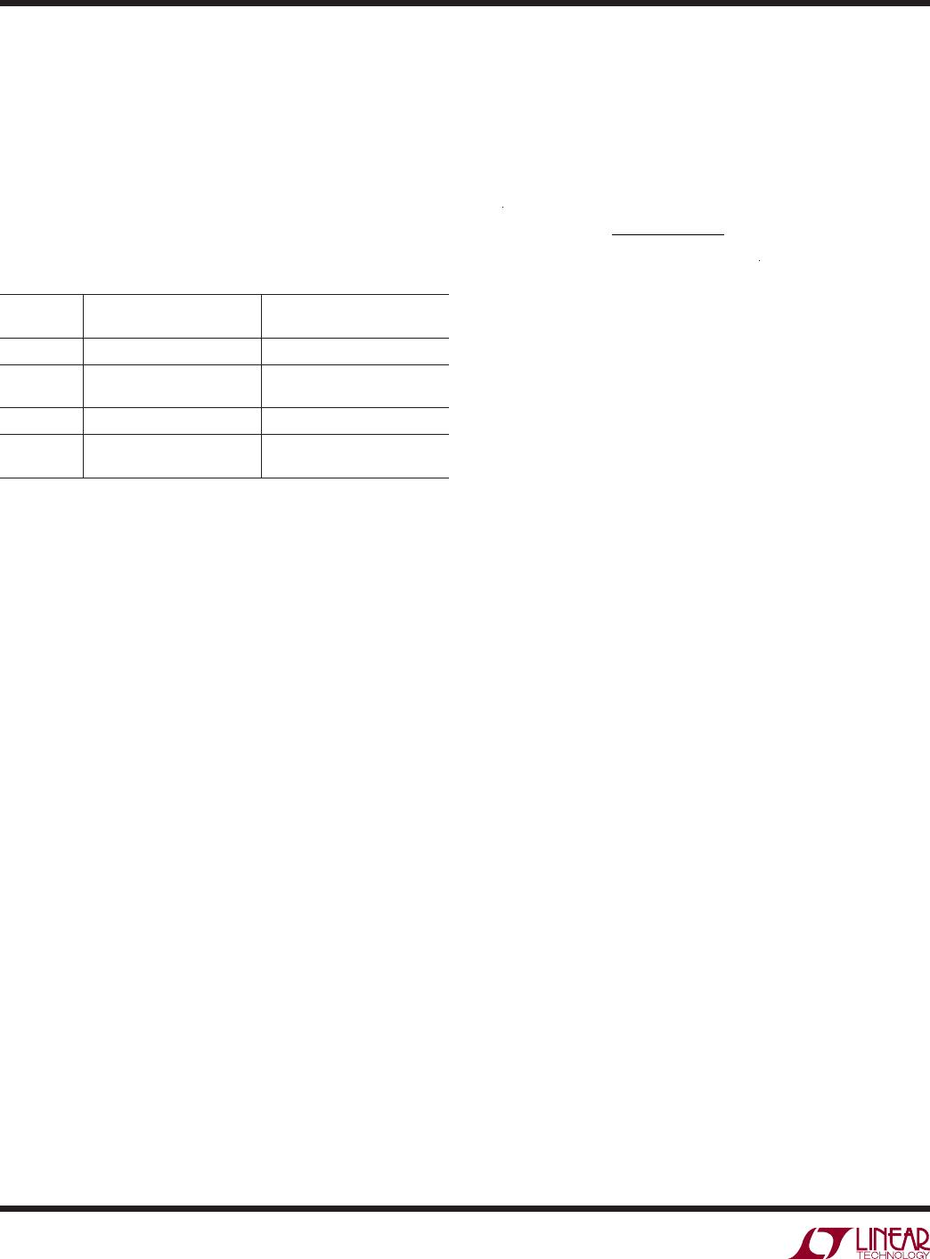
Several series of inductors that work well with the LT3582
series are listed in Table 3. This table is not complete, and
there are many other manufacturers and parts that can
be used. Consult each manufacturer for more detailed
information and for their entire selection of related parts,
as many different sizes and shapes are available.
Table 3. Inductor Manufacturers
Coilcraft LPS3008-LPS4018 Series,
XPL2010 Series
www.coilcraft.com
Murata LQH32C, LQH43C Series www.murata.com
Sumida CDRH26D09, CDRH26D11,
CDRH3D14 Series
www.sumida.com
TDK VLF and VLCF Series www.tdk.com
Würth
Elektronik
WE-TPC Series Type T, TH,
XS and S
www.we-online.com
Inductances of 2.2H to 10µH typically result in a good
tradeoff between inductor size and system performance.
More inductance typically yields an increase in effi ciency
at the expense of increased output ripple. Less inductance
may be used in a given application depending on required
effi ciency and output current. For higher effi ciency, choose
inductors with high frequency core material, such as ferrite,
to reduce core losses. Also to improve effi ciency, choose
inductors with more volume for a given inductance. The
inductor should have low DCR (copper-wire resistance)
to reduce I
2
R losses, and must be able to handle the peak
inductor current without saturating. To minimize radiated
noise, use a toroidal or shielded inductor (note that the
inductance of shielded types will drop more as current
increases, and will saturate more easily).
Peak Current Rating: Real inductors can experience a drop
in inductance as current and temperature increase. The
inductors should have saturation current ratings higher
than the peak inductor currents. The peak inductor cur-
rents can be calculated as:
I
PK
I
LIMIT
+
V
LSWON
T
OS
L
mA
where:
I
PK
= Peak inductor current
I
LIMIT
= Typically 350mA for Boost and 600mA
for Inverting
L = Inductance in µH
V
LSWON
= Maximum inductor voltage when the
power switch is “on.” Typically max V
IN
for the Boost and Inverting converters.
T
OS
= 100 for Boost and 125 for Inverting
APPLICATIONS INFORMATION

LT3582EUD-5#TRPBF

Mfr. #:
Manufacturer:
Analog Devices / Linear Technology
Description:
Switching Voltage Regulators Programmable Boost and Single Inductor Inverting DC/DC Converters with OTP
Lifecycle:
New from this manufacturer.
Delivery:
DHL FedEx Ups TNT EMS
Payment:
T/T Paypal Visa MoneyGram Western Union