AD7730/AD7730L
–13–
Communications Register (RS2–RS0 = 0, 0, 0)
The Communications Register is an 8-bit write-only register. All communications to the part must start with a write operation to the
Communications Register. The data written to the Communications Register determines whether the next operation is a read or
write operation, the type of read operation, and to which register this operation takes place. For single-shot read or write operations,
once the subsequent read or write operation to the selected register is complete, the interface returns to where it expects a write op-
eration to the Communications Register. This is the default state of the interface, and on power-up or after a RESET, the AD7730
is in this default state waiting for a write operation to the Communications Register. In situations where the interface sequence is
lost, a write operation of at least 32 serial clock cycles with DIN high, returns the AD7730 to this default state by resetting the
part. Table VI outlines the bit designations for the Communications Register. CR0 through CR7 indicate the bit location, CR denot-
ing the bits are in the Communications Register. CR7 denotes the first bit of the data stream.
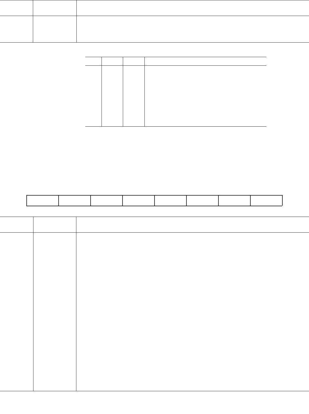
Table VI. Communications Register
CR7 CR6 CR5 CR4 CR3 CR2 CR1 CR0
WEN ZERO RW1 RW0 ZERO RS2 RS1 RS0
Bit Bit
Location Mnemonic Description
CR7 WEN Write Enable Bit. A 0 must be written to this bit so the write operation to the Communications
Register actually takes place. If a 1 is written to this bit, the part will not clock on to subsequent
bits in the register. It will stay at this bit location until a 0 is written to this bit. Once a 0 is writ-
ten to the WEN bit, the next seven bits will be loaded to the Communications Register.
CR6 ZERO A zero must be written to this bit to ensure correct operation of the AD7730.
CR5, CR4 RW1, RW0 Read/Write Mode Bits. These two bits determine the nature of the subsequent read/write opera-
tion. Table VII outlines the four options.
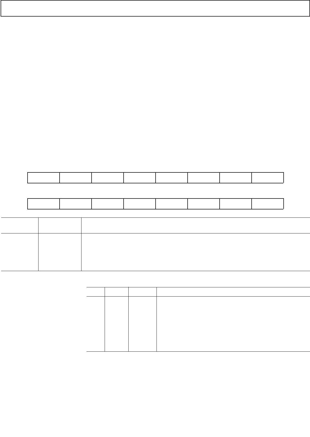
Table VII. Read/Write Mode
RW1 RW0 Read/Write Mode
0 0 Single Write to Specified Register
0 1 Single Read of Specified Register
1 0 Start Continuous Read of Specified Register
1 1 Stop Continuous Read Mode
With 0, 0 written to these two bits, the next operation is a write operation to the register specified by
bits RS2, RS1, RS0. Once the subsequent write operation to the specified register has been com-
pleted, the part returns to where it is expecting a write operation to the Communications Register.
With 0,1 written to these two bits, the next operation is a read operation of the register specified
by bits RS2, RS1, RS0. Once the subsequent read operation to the specified register has been
completed, the part returns to where it is expecting a write operation to the Communications
Register.
Writing 1,0 to these bits, sets the part into a mode of continuous reads from the register speci-
fied by bits RS2, RS1, RS0. The most likely registers with which the user will want to use this
function are the Data Register and the Status Register. Subsequent operations to the part will
consist of read operations to the specified register without any intermediate writes to the Com-
munications Register. This means that once the next read operation to the specified register has
taken place, the part will be in a mode where it is expecting another read from that specified
register. The part will remain in this continuous read mode until 30 Hex has been written to the
Communications Register.
When 1,1 is written to these bits (and 0 written to bits CR3 through CR0), the continuous read
mode is stopped and the part returns to where it is expecting a write operation to the Communi-
cations Register. Note, the part continues to look at the DIN line on each SCLK edge during
continuous read mode to determine when to stop the continuous read mode. Therefore, the user
must be careful not to inadvertently exit the continuous read mode or reset the AD7730 by
writing a series of 1s to the part. The easiest way to avoid this is to place a logic 0 on the DIN
line while the part is in continuous read mode. Once the part is in continuous read mode, the
user should ensure that an integer multiple of 8 serial clocks should have taken place before
attempting to take the part out of continuous read mode.
REV. B
AD7730/AD7730L
–14–
Bit Bit
Location Mnemonic Description
CR3 ZERO A zero must be written to this bit to ensure correct operation of the AD7730.
CR2–CR0 RS2–RS0 Register Selection Bits. RS2 is the MSB of the three selection bits. The three bits select
which register type the next read or write operation operates upon as shown in Table VIII.
Table VIII. Register Selection
RS2 RS1 RS0 Register
0 0 0 Communications Register (Write Operation)
0 0 0 Status Register (Read Operation)
0 0 1 Data Register
0 1 0 Mode Register
0 1 1 Filter Register
1 0 0 DAC Register
1 0 1 Offset Register
1 1 0 Gain Register
1 1 1 Test Register
Status Register (RS2–RS0 = 0, 0, 0); Power-On/Reset Status: CX Hex
The Status Register is an 8-bit read-only register. To access the Status Register, the user must write to the Communications Register
selecting either a single-shot read or continuous read mode and load bits RS2, RS1, RS0 with 0, 0, 0. Table IX outlines the bit desig-
nations for the Status Register. SR0 through SR7 indicate the bit location, SR denoting the bits are in the Status Register. SR7
denotes the first bit of the data stream. Figure 5 shows a flowchart for reading from the registers on the AD7730. The number
in brackets indicates the power-on/reset default status of that bit.
Table IX. Status Register
SR7 SR6 SR5 SR4 SR3 SR2 SR1 SR0
RDY (1) STDY (1) STBY (0) NOREF (0) MS3 (X) MS2 (X) MS1 (X) MS0 (X)
Bit Bit
Location Mnemonic Description
SR7 RDY Ready Bit. This bit provides the status of the RDY flag from the part. The status and function of
this bit is the same as the RDY output pin. A number of events set the RDY bit high as indi-
cated in Table XVIII.
SR6 STDY Steady Bit. This bit is updated when the filter writes a result to the Data Register. If the filter is
in
FASTStep
mode (see Filter Register section) and responding to a step input, the STDY bit
remains high as the initial conversion results become available. The RDY output and bit are set
low on these initial conversions to indicate that a result is available. If the STDY is high, however,
it indicates that the result being provided is not from a fully settled second-stage FIR filter. When the
FIR filter has fully settled, the STDY bit will go low coincident with RDY. If the part is never placed
into its
FASTStep
mode, the STDY bit will go low at the first Data Register read and it is
not cleared by subsequent Data Register reads.
A number of events set the STDY bit high as indicated in Table XVIII. STDY is set high along
with RDY by all events in the table except a Data Register read.
SR5 STBY Standby Bit. This bit indicates whether the AD7730 is in its Standby Mode or normal mode of
operation. The part can be placed in its standby mode using the STANDBY input pin or by
writing 011 to the MD2 to MD0 bits of the Mode Register. The power-on/reset status of this bit
is 0 assuming the STANDBY pin is high.
SR4 NOREF No Reference Bit. If the voltage between the REF IN(+) and REF IN(–) pins is below 0.3 V, or
either of these inputs is open-circuit, the NOREF bit goes to 1. If NOREF is active on comple-
tion of a conversion, the Data Register is loaded with all 1s. If NOREF is active on completion
of a calibration, updating of the calibration registers is inhibited.
SR3–SR0 MS3–MS0 These bits are for factory use. The power-on/reset status of these bits vary, depending on the
factory-assigned number.
REV. B
AD7730/AD7730L
–15–
Data Register (RS2–RS0 = 0, 0, 1); Power On/Reset Status: 000000 Hex
The Data Register on the part is a read-only register which contains the most up-to-date conversion result from the AD7730. Fig-
ure 5 shows a flowchart for reading from the registers on the AD7730. The register can be programmed to be either 16 bits or 24bits
wide, determined by the status of the WL bit of the Mode Register. The RDY output and RDY bit of the Status Register are set low
when the Data Register is updated. The RDY pin and RDY bit will return high once the full contents of the register (either 16 bits or
24 bits) have been read. If the Data Register has not been read by the time the next output update occurs, the RDY pin and RDY bit
will go high for at least 100 × t
CLK IN
, indicating when a read from the Data Register should not be initiated to avoid a transfer from
the Data Register as it is being updated. Once the updating of the Data Register has taken place, RDY returns low.
If the Communications Register data sets up the part for a write operation to this register, a write operation must actually take place
in order to return the part to where it is expecting a write operation to the Communications Register (the default state of the inter-
face). However, the 16 or 24 bits of data written to the part will be ignored by the AD7730.
Mode Register (RS2–RS0 = 0, 1, 0); Power On/Reset Status: 01B0 Hex
The Mode Register is a 16-bit register from which data can be read or to which data can be written. This register configures
the operating modes of the AD7730, the input range selection, the channel selection and the word length of the Data Register.
Table X outlines the bit designations for the Mode Register. MR0 through MR15 indicate the bit location, MR denoting the bits are
in the Mode Register. MR15 denotes the first bit of the data stream. The number in brackets indicates the power-on/reset default
status of that bit. Figure 5 shows a flowchart for reading from the registers on the AD7730 and Figure 6 shows a flowchart for writ-
ing to the registers on the part.
Table X. Mode Register
MR15 MR14 MR13 MR12 MR11 MR10 MR9 MR8
MD2 (0) MD1 (0) MD0 (0) B/U (0) DEN (0) D1 (0) D0 (0) WL (1)
MR7 MR6 MR5 MR4 MR3 MR2 MR1 MR0
HIREF (1) ZERO (0) RN1 (1) RN0 (1) CLKDIS (0) BO (0) CH1 (0) CH0 (0)
Bit Bit
Location Mnemonic Description
MR15–MR13 MD2–MD0 Mode Bits. These three bits determine the mode of operation of the AD7730 as outlined in
Table XI. The modes are independent, such that writing new mode bits to the Mode Register
will exit the part from the mode in which it is operating and place it in the new requested mode
immediately after the Mode Register write. The function of the mode bits is described in more
detail below.
Table XI. Operating Modes
MD2 MD1 MD0 Mode of Operation
0 0 0 Sync (Idle) Mode Power-On/Reset Default
0 0 1 Continuous Conversion Mode
0 1 0 Single Conversion Mode
0 1 1 Power-Down (Standby) Mode
1 0 0 Internal Zero-Scale Calibration
1 0 1 Internal Full-Scale Calibration
1 1 0 System Zero-Scale Calibration
1 1 1 System Full-Scale Calibration
REV. B

AD7730LBRUZ-REEL7

Mfr. #:
Manufacturer:
Analog Devices Inc.
Description:
Analog to Digital Converters - ADC CMOS 24-Bit Low Pwr
Lifecycle:
New from this manufacturer.
Delivery:
DHL FedEx Ups TNT EMS
Payment:
T/T Paypal Visa MoneyGram Western Union