AD7730/AD7730L
–31–
user must write either 0, 0, 1 or 0, 1, 0 to the MD2, MD1,
MD0 bits of the Mode Register to initiate a conversion. If
RDY is low before (or goes low during) the calibration com-
mand write to the Mode Register, it may take up to one modulator
cycle (MCLK IN/32) before RDY goes high to indicate that
calibration is in progress. Therefore, RDY should be ignored for
up to one modulator cycle after the last bit of the calibration
command is written to the Mode Register.
System Zero-Scale Calibration
System calibration allows the AD7730 to compensate for system
gain and offset errors as well as its own internal errors. System
calibration performs the same slope factor calculations as self-
calibration, but uses voltage values presented by the system to
the AIN inputs for the zero- and full-scale points.
A system zero-scale calibration is initiated on the AD7730 by
writing the appropriate values (1, 1, 0) to the MD2, MD1 and
MD0 bits of the Mode Register. In this calibration mode, with a
unipolar input range, the zero-scale point used in determin-
ing the calibration coefficients is the bottom end of the trans-
fer function. The system’s zero-scale point is applied to the
AD7730’s AIN input before the calibration step and this voltage
must remain stable for the duration of the system zero-scale
calibration. The PGA is set for the selected gain (as per the
RN1, RN0 bits in the Mode Register) for this system zero-scale
calibration conversion. The allowable range for the system zero-
scale voltage is discussed in the Span and Offsets Section.
The calibration is performed with either ac or dc excitation,
depending on the status of the AC bit. The duration time of the
calibration depends upon the CHP bit of the Filter Register.
With CHP = 1, the duration is 22 × 1/Output Rate; with
CHP = 0, the duration is 24 × 1/Output Rate. At this time the
MD2, MD1 and MD0 bits in the Mode Register return to
0, 0, 0 (Sync or Idle Mode for the AD7730). The RDY line
goes high when calibration is initiated and returns low when
calibration is complete. Note that the part has not performed a
conversion at this time; it has simply performed a zero-scale
calibration and updated the Offset Calibration Register for the
selected channel. The user must write either 0, 0, 1 or 0, 1, 0 to
the MD2, MD1, MD0 bits of the Mode Register to initiate a
conversion. If RDY is low before (or goes low during) the cali-
bration command write to the Mode Register, it may take up to
one modulator cycle (MCLK IN/32) before RDY goes high to
indicate that calibration is in progress. Therefore, RDY should
be ignored for up to one modulator cycle after the last bit of the
calibration command is written to the Mode Register.
For bipolar input ranges in the system zero-scale calibrating
mode, the sequence is very similar to that just outlined. In this
case, the zero-scale point is the midpoint of the AD7730’s
transfer function.
The system zero-scale calibration needs to be performed as one
part of a two part full calibration. However, once a full calibra-
tion has been performed, additional system zero-scale calibra-
tions can be performed by themselves to adjust the part’s
zero-scale point only. When performing a two-step full calibra-
tion care should be taken as to the sequence in which the two
steps are performed. If the system zero-scale calibration is one
part of a full system calibration, then it should take place before
a system full-scale calibration. If it takes place in association
with an internal full-scale calibration, then this system zero-scale
calibration should be performed after the full-scale calibration.
System Full-Scale Calibration
A system full-scale calibration is initiated on the AD7730 by
writing the appropriate values (1, 1, 1) to the MD2, MD1 and
MD0 bits of the Mode Register. System full-scale calibration is
performed using the system's positive full-scale voltage. This
full-scale voltage must be set up before the calibration is initi-
ated, and it must remain stable throughout the calibration step.
The system full-scale calibration is performed at the selected
gain (as per the RN1, RN0 bits in the Mode Register).
The calibration is performed with either ac or dc excitation,
depending on the status of the ac bit. The duration time of the
calibration depends upon the CHP bit of the Filter Register.
With CHP = 1, the duration is 22 × 1/Output Rate; with CHP =
0, the duration is 24 × 1/Output Rate. At this time the MD2,
MD1 and MD0 bits in the Mode Register return to 0, 0, 0
(Sync or Idle Mode for the AD7730). The RDY line goes high
when calibration is initiated, and returns low when calibration is
complete. Note that the part has not performed a conversion at
this time; it has simply performed a full-scale calibration and
updated the Gain Calibration Register for the selected channel.
The user must write either 0, 0, 1 or 0, 1, 0 to the MD2, MD1,
MD0 bits of the Mode Register to initiate a conversion. If RDY
is low before (or goes low during) the calibration command
write to the Mode Register, it may take up to one modulator
cycle (MCLK IN/32) before RDY goes high to indicate that
calibration is in progress. Therefore, RDY should be ignored for
up to one modulator cycle after the last bit of the calibration
command is written to the Mode Register.
The system full-scale calibration needs to be performed as one
part of a two part full calibration. Once a full calibration has
been performed, however, additional system full-scale calibra-
tions can be performed by themselves to adjust the part's gain
calibration point only. When performing a two-step full calibra-
tion care should be taken as to the sequence in which the two
steps are performed. A system full-scale calibration should not
be carried out unless the part contains valid zero-scale coeffi-
cients. Therefore, an internal zero-scale calibration or a system
zero-scale calibration must be performed before the system full-
scale calibration when a full two-step calibration operation is
being performed.
Span and Offset Limits
Whenever a system calibration mode is used, there are limits
on the amount of offset and span which can be accommodated.
The overriding requirement in determining the amount of offset
and gain which can be accommodated by the part is the require-
ment that the positive full-scale calibration limit is
1.05 × FS,
where FS is 10 mV, 20 mV, 40 mV or 80 mV depending on the
RN1, RN0 bits in the Mode Register. This allows the input
range to go 5% above the nominal range. The built-in head-
room in the AD7730’s analog modulator ensures that the part
will still operate correctly with a positive full-scale voltage that is
5% beyond the nominal.
REV. B
AD7730/AD7730L
–32–
The range of input span in both the unipolar and bipolar modes
has a minimum value of 0.8 × FS and a maximum value of
2.1 × FS. However, the span (which is the difference between
the bottom of the AD7730’s input range and the top of its input
range) has to take into account the limitation on the positive
full-scale voltage. The amount of offset which can be accommo-
dated depends on whether the unipolar or bipolar mode is being
used. Once again, the offset has to take into account the limita-
tion on the positive full-scale voltage. In unipolar mode, there is
considerable flexibility in handling negative (with respect to
AIN(–)) offsets. In both unipolar and bipolar modes, the range
of positive offsets that can be handled by the part depends on
the selected span. Therefore, in determining the limits for sys-
tem zero-scale and full-scale calibrations, the user has to ensure
that the offset range plus the span range does exceed 1.05 × FS.
This is best illustrated by looking at a few examples.
If the part is used in unipolar mode with a required span of
0.8 × FS, the offset range the system calibration can handle is
from –1.05 × FS to +0.25 × FS. If the part is used in unipolar
mode with a required span of FS, the offset range the system cali-
bration can handle is from –1.05 × FS to +0.05 × FS. Similarly, if
the part is used in unipolar mode and required to remove an
offset of 0.2 × FS, the span range the system calibration can
handle is 0.85 × FS.
If the part is used in bipolar mode with a required span of
± 0.4 × FS, the offset range the system calibration can handle is
from –0.65 × FS to +0.65 × FS. If the part is used in bipolar
mode with a required span of ± FS, the offset range the system
calibration can handle is from –0.05 × FS to +0.05 × FS. Simi-
larly, if the part is used in bipolar mode and required to remove
an offset of ±0.2 × FS, the span range the system calibration can
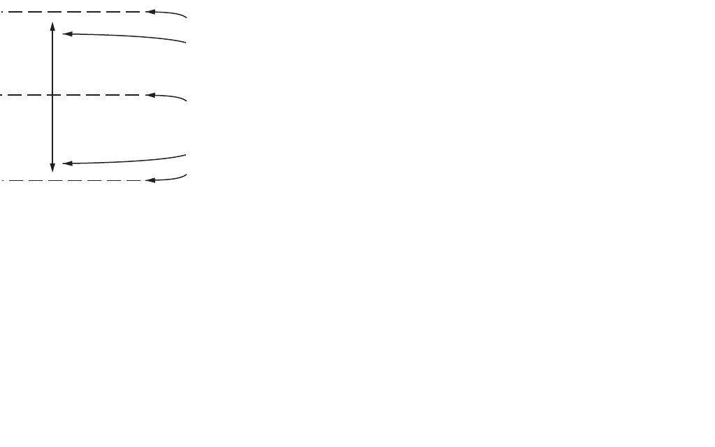
handle is ± 0.85 × FS. Figure 16 summarizes the span and offset
ranges.
UPPER LIMIT. AD7730’s INPUT
VOLTAGE CANNOT EXCEED THIS
0V DIFFERENTIAL
1.05 FS.
NOMINAL ZERO-SCALE POINT
–1.05FS.
LOWER LIMIT. AD7730’s INPUT
VOLTAGE CANNOT EXCEED THIS
AD7730
INPUT RANGE
(0.8 FS TO
2.1FS)
GAIN CALIBRATIONS EXPAND OR
CONTRACT THE AD7730’s INPUT
RANGE
ZERO-SCALE CALIBRATIONS
MOVE INPUT RANGE UP OR DOWN
Figure 16. Span and Offset Limits
Power-Up and Calibration
On power-up, the AD7730 performs an internal reset which sets
the contents of the internal registers to a known state. There are
default values loaded to all registers after a power-on or reset.
The default values contain nominal calibration coefficients for
the calibration registers. To ensure correct calibration for the
device, a calibration routine should be performed after power-up.
The power dissipation and temperature drift of the AD7730 are
low and no warm-up time is required before the initial calibra-
tion is performed. If, however, an external reference is being
used, this reference must have stabilized before calibration is
initiated. Similarly, if the clock source for the part is generated
from a crystal or resonator across the MCLK pins, the start-up
time for the oscillator circuit should elapse before a calibration
is initiated on the part (see below).
Drift Considerations
The AD7730 uses chopper stabilization techniques to minimize
input offset drift. Charge injection in the analog multiplexer and
dc leakage currents at the analog input are the primary sources
of offset voltage drift in the part. The dc input leakage current is
essentially independent of the selected gain. Gain drift within
the converter depends primarily upon the temperature tracking
of the internal capacitors. It is not affected by leakage currents.
When operating the part in CHOP mode (CHP = 1), the signal
chain including the first-stage filter is chopped. This chopping
reduces the overall offset drift to 5 nV/°C. Integral and differen-
tial linearity errors are not significantly affected by temperature
changes.
Care must also be taken with external drift effects in order to
achieve optimum drift performance. The user has to be espe-
cially careful to avoid, as much as possible, thermocouple effects
from junctions of different materials. Devices should not be
placed in sockets when evaluating temperature drift, there
should be no links in series with the analog inputs and care
must be taken as to how the input voltage is applied to the input
pins. The true offset drift of the AD7730 itself can be evaluated
by performing temperature drift testing of the part with the
AIN(–)/AIN(–) input channel arrangement (i.e., internal shorted
input, test mode).
USING THE AD7730
Clocking and Oscillator Circuit
The AD7730 requires a master clock input, which may be an
external CMOS compatible clock signal applied to the MCLK IN
pin with the MCLK OUT pin left unconnected. Alternatively, a
crystal or ceramic resonator of the correct frequency can be
connected between MCLK IN and MCLK OUT in which case
the clock circuit will function as an oscillator, providing the
clock source for the part. The input sampling frequency, the
modulator sampling frequency, the –3 dB frequency, output
update rate and calibration time are all directly related to the
master clock frequency, f
CLK IN
. Reducing the master clock
frequency by a factor of two will halve the above frequencies and
update rate and double the calibration time.
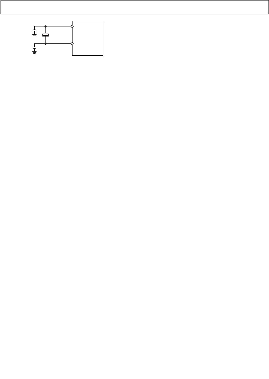
The crystal or ceramic resonator is connected across the MCLK
IN and MCLK OUT pins, as per Figure 17. Capacitors C1 and
C2 may or may not be required and may vary in value depend-
ing on the crystal/resonator manufacturer's recommendations.
The AD7730 has a capacitance of 5 pF on MCLK IN and 13 pF
on MCLK OUT so, in most cases, capacitors C1 and C2 will
not be required to get the crystal/resonator operating at its cor-
rect frequency.
REV. B
AD7730/AD7730L
–33–
AD7730
CRYSTAL OR
CERAMIC
RESONATOR
C1
C2
MCLK IN
MCLK OUT
Figure 17. Crystal/Resonator Connections
The on-chip oscillator circuit also has a start-up time associated
with it before it has attained its correct frequency and correct
voltage levels. The typical start-up time for the circuit is 6 ms,
with a DV
DD
of +5 V and 8 ms with a DV
DD
of +3 V.
The AD7730’s master clock appears on the MCLK OUT pin of
the device. The maximum recommended load on this pin is one
CMOS load. When using a crystal or ceramic resonator to gen-
erate the AD7730’s clock, it may be desirable to then use this
clock as the clock source for the system. In this case, it is recom-
mended that the MCLK OUT signal is buffered with a CMOS
buffer before being applied to the rest of the circuit.
System Synchronization
The SYNC input allows the user to reset the modulator and
digital filter without affecting any of the setup conditions on the
part. This allows the user to start gathering samples of the ana-
log input from a known point in time, i.e., the rising edge of
SYNC.
If multiple AD7730s are operated from a common master clock,
they can be synchronized to update their output registers simul-
taneously. A falling edge on the SYNC input resets the digital
filter and analog modulator and places the AD7730 into a con-
sistent, known state. While the SYNC input is low, the AD7730
will be maintained in this state. On the rising edge of SYNC,
the modulator and filter are taken out of this reset state and on
the next clock edge the part starts to gather input samples again.
In a system using multiple AD7730s, a common signal to their
SYNC inputs will synchronize their operation. This would nor-
mally be done after each AD7730 has performed its own cali-
bration or has had calibration coefficients loaded to it. The
output updates will then be synchronized with the maximum
possible difference between the output updates of the individual
AD7730s being one MCLK IN cycle.
Single-Shot Conversions
The SYNC input can also be used as a start convert command
allowing the AD7730 to be operated in a conventional converter
fashion. In this mode, the rising edge of SYNC starts conversion
and the falling edge of RDY indicates when conversion is com-
plete. The disadvantage of this scheme is that the settling time
of the filter has to be taken into account for every data register
update.
Writing 0, 1, 0 to the MD2, MD1, MD0 bits of the Mode regis-
ter has the same effect. This initiates a single conversion on the
AD7730 with the part returning to idle mode at the end of
conversion. Once again, the full settling-time of the filter has to
elapse before the Data Register is updated.
Reset Input
The RESET input on the AD7730 resets all the logic, the digital
filter and the analog modulator while all on-chip registers are
reset to their default state. RDY is driven high and the AD7730
ignores all communications to any of its registers while the
RESET input is low. When the RESET input returns high, the
AD7730 starts to process data and RDY will return low after
the filter has settled indicating a valid new word in the data
register. However, the AD7730 operates with its default setup
conditions after a RESET and it is generally necessary to set up all
registers and carry out a calibration after a RESET command.
The AD7730’s on-chip oscillator circuit continues to function
even when the RESET input is low. The master clock signal
continues to be available on the MCLK OUT pin. Therefore, in
applications where the system clock is provided by the AD7730’s
clock, the AD7730 produces an uninterrupted master clock
during RESET commands.
Standby Mode
The STANDBY input on the AD7730 allows the user to place
the part in a power-down mode when it is not required to pro-
vide conversion results. The part can also be placed in its
standby mode by writing 0, 1, 1 to the MD2, MD1, MD0 bits
of the Mode Register. The AD7730 retains the contents of all its
on-chip registers (including the Data Register) while in standby
mode. Data can still be read from the part in Standby Mode.
The STBY bit of the Status Register indicates whether the part
is in standby or normal operating mode. When the STANDBY
pin is taken high, the part returns to operating as it had been
prior to the STANDBY pin going low.
The STANDBY input (or 0, 1, 1 in the MD2, MD1, MD0 bits)
does not affect the digital interface. It does, however, set the
RDY bit and pin high and also sets the STDY bit high. When
STANDBY goes high again, RDY and STDY remain high until
set low by a conversion or calibration.
Placing the part in standby mode, reduces the total current to
10 μA typical when the part is operated from an external master
clock provided this master clock is stopped. If the external clock
continues to run in standby mode, the standby current increases
to 400 μA typical. If a crystal or ceramic resonator is used as the
clock source, then the total current in standby mode is 400 μA
typical. This is because the on-chip oscillator circuit continues
to run when the part is in its standby mode. This is important in
applications where the system clock is provided by the AD7730’s
clock, so that the AD7730 produces an uninterrupted master
clock even when it is in its standby mode.
Digital Outputs
The AD7730 has two digital output pins, D0 and D1. When the
DEN bit of the Mode Register is set to 1, these digital outputs
assume the logic status of bits D0 and D1 of the Mode Register.
It gives the user access to two digital port pins which can be
programmed over the normal serial interface of the AD7730.
The two outputs obtain their supply voltage from AV
DD
,
thus the outputs operate to 5 V levels even in cases where
DV
DD
= +3 V.
REV. B

AD7730LBRUZ-REEL7

Mfr. #:
Manufacturer:
Analog Devices Inc.
Description:
Analog to Digital Converters - ADC CMOS 24-Bit Low Pwr
Lifecycle:
New from this manufacturer.
Delivery:
DHL FedEx Ups TNT EMS
Payment:
T/T Paypal Visa MoneyGram Western Union