AD7730/AD7730L
–25–
Burnout Currents
The AD7730 contains two 100 nA constant current generators,
one source current from AV
DD
to AIN(+) and one sink current
from AIN(–) to AGND. The currents are switched to the se-
lected analog input pair. Both currents are either on or off,
depending on the BO bit of the Mode Register. These currents
can be used in checking that a transducer is still operational
before attempting to take measurements on that channel. If the
currents are turned on, allowed flow in the transducer, a mea-
surement of the input voltage on the analog input taken and the
voltage measured is full scale, it indicates that the transducer
has gone open-circuit. If the voltage measured is 0 V, it indicates
that the transducer has gone short circuit. For normal operation,
these burnout currents are turned off by writing a 0 to the BO
bit. The current sources work over the normal absolute input
voltage range specifications.
REFERENCE INPUT
The AD7730’s reference inputs, REF IN(+) and REF IN(–),
provide a differential reference input capability. The common-
mode range for these differential inputs is from AGND to
AV
DD
. The nominal reference voltage, V
REF
(REF IN(+)—
REF IN(–)), for specified operation is +2.5 V with the HIREF
bit at 0 V and +5 V with the HIREF bit at 1. The part is also
functional with V
REF
of +2.5 V with the HIREF bit at 1. This
results in a halving of all input ranges. The resolution in nV will
be unaltered but will appear halved in terms of counts.
Both reference inputs provide a high impedance, dynamic load.
The typical average dc input leakage current over temperature
is 8.5 μA with HIREF = 1 and V
REF
= +5 V, and 2.5 μA with
HIREF = 0 and V
REF
= +2.5 V. Because the input impedance of
each reference input is dynamic, external resistance/capacitance
combinations on these inputs may result in gain errors on the
part.
The AD7730 can be operated in either ac or dc mode. If the
bridge excitation is fixed dc, the AD7730 should be operated in
dc mode. If the analog input and the reference inputs are externally
chopped before being applied to the part the AD7730 should be
operated in ac mode and not dc mode. In ac mode, it is assumed
that both the analog inputs and reference inputs are chopped
and as a result change phase every alternate chopping cycle. If
the chopping is synchronized by the AD7730 (using the ACX
signals to control the chopping) the part then takes into account
the reversal of the analog input and reference input signals.
The output noise performance outlined in Tables I through IV
is for an analog input of 0 V and is unaffected by noise on the
reference. To obtain the same noise performance as shown in
the noise tables over the full input range requires a low noise
reference source for the AD7730. If the reference noise in the
bandwidth of interest is excessive, it will degrade the performance
of the AD7730. In applications where the excitation voltage for
the bridge transducer on the analog input also drives the refer-
ence voltage for the part, the effect of the noise in the excita-
tion voltage will be removed as the application is ratiometric.
Figure 7 shows how the reference voltage can be connected in a
ratiometric fashion in a dc-excited bridge application. In this
case, the excitation voltage for the AD7730 and the transducer
is a dc voltage. The HIREF bit of the Mode Register should be
set to 1. Figure 8 meanwhile shows how the reference can be
connected in a ratiometric fashion in an ac-excited bridge
AV
DD
DV
DD
AGND DGND
AD7730
EXCITATION
VOLTAGE = +5V
IN+
OUT–
IN–
OUT+
REF IN(+)
REF IN(–)
AIN1(+)
AIN1(–)
Figure 7. Ratiometric Generation of Reference in DC-
Excited Bridge Application
AV
DD
DV
DD
EXCITATION
VOLTAGE = +5V
AGND DGND
IN+
OUT–
IN–
OUT+
AD7730
REF IN(+)
REF IN(–)
AIN1(+)
AIN1(–)
ACX
ACX
AC
EXCITATION
CLOCK
Figure 8. Ratiometric Generation of Reference in AC-
Excited Bridge Application
application. In this case, both the reference voltage for the part
and the excitation voltage for the transducer are chopped. Once
again, the HIREF bit should be set to 1.
If the AD7730 is not used in a ratiometric application, a low
noise reference should be used. Recommended 2.5 V reference
voltage sources for the AD7730 include the AD780, REF43
and REF192. If any of these references are used as the reference
source for the AD7730, the HIREF bit should be set to 0. It is
generally recommended to decouple the output of these references
to further reduce the noise level.
Reference Detect
The AD7730 includes on-chip circuitry to detect if the part
has a valid reference for conversions or calibrations. If the volt-
age between the REF IN(+) and REF IN(–) pins goes below
0.3 V or either the REF IN(+) or REF IN(–) inputs is open
circuit, the AD7730 detects that it no longer has a valid reference.
In this case, the NO REF bit of the Status Register is set to a 1.
If the AD7730 is performing normal conversions and the NO
REF bit becomes active, the part places all ones in the Data
Register. Therefore, it is not necessary to continuously monitor
the status of the NO REF bit when performing conversions. It is
only necessary to verify its status if the conversion result read
from the Data Register is all 1s.
REV. B
AD7730/AD7730L
–26–
If the AD7730 is performing either an offset or gain calibration
and the NOREF bit becomes active, the updating of the respec-
tive calibration register is inhibited to avoid loading incorrect
coefficients to this register. If the user is concerned about verify-
ing that a valid reference is in place every time a calibration is
performed, then the status of the NOREF bit should be checked
at the end of the calibration cycle.
SIGMA-DELTA MODULATOR
A sigma-delta ADC generally consists of two main blocks, an
analog modulator and a digital filter. In the case of the AD7730,
the analog modulator consists of a difference amplifier, an inte-
grator block, a comparator and a feedback DAC as illustrated in
Figure 9. In operation, the analog signal sample is fed to the
difference amplifier along with the output of the feedback DAC.
The difference between these two signals is integrated and fed to
the comparator. The output of the comparator provides the
input to the feedback DAC so that the system functions as a
negative feedback loop that tries to minimize the difference
signal. The digital data that represents the analog input voltage
is contained in the duty cycle of the pulse train appearing at the
output of the comparator. This duty cycle data can be recovered
as a data word using the digital filter. The sampling frequency of
the modulator loop is many times higher than the bandwidth of
the input signal. The integrator in the modulator shapes the
quantization noise (which results from the analog-to-digital
conversion) so that the noise is pushed toward one half of the
modulator frequency. The digital filter then bandlimits the re-
sponse to a frequency significantly lower than one half of the
modulator frequency. In this manner, the 1-bit output of the
comparator is translated into a bandlimited, low noise output
from the AD7730.
DAC
INTEGRATOR
ANALOG
INPUT
DIFFERENCE
AMP
COMPARATOR
DIGITAL
FILTER
DIGITAL DATA
Figure 9. Sigma-Delta Modulator Block Diagram
DIGITAL FILTERING
Filter Architecture
The output of the modulator feeds directly into the digital filter.
This digital filter consists of two portions, a first stage filter and
a second stage filter. The first stage filter is a sinc
3
, low-pass
filter. The cutoff frequency and output rate of this first stage
filter is programmable. The second stage filter has three distinct
modes of operation. In its normal mode, it provides a low-pass
FIR filter that processes the output of the first stage filter. When
a step change is detected on the analog input, this second stage
filter enters a second mode where it performs a variable number
of averages for some time after the step change and then the
second stage filter switches back to the FIR filter. The third
option for the second stage filter is that it is completely bypassed
so the only filtering provided on the AD7730 is the first stage.
The various filter stages and options are discussed in the follow-
ing sections.
First Stage Filter
The first stage filter is a low-pass, sinc
3
or (sinx/x)
3
filter whose
primary function is to remove the quantization noise introduced
at the modulator. The cutoff frequency and output rate of this
filter is programmed via the SF0 to SF11 bits of the Filter Reg-
ister. The frequency response for this first stage filter is shown in
Figure 10. The response of this first stage filter is similar to that
of an averaging filter but with a sharper roll-off. The output rate
for the filter corresponds with the positioning of the first notch
of the filter’s frequency response. Thus, for the plot of Figure 10,
where the output rate is 600 Hz (f
CLK IN
= 4.9152 MHz and
SF = 512), the first notch of the filter is at 600 Hz. The notches
of this sinc
3
filter are repeated at multiples of the first notch. The
filter provides attenuation of better than 100 dB at these notches.
Programming a different cutoff frequency via SF0 – SF11 does
not alter the profile of the filter response; it changes the fre-
quency of the notches as outlined in the Filter Registers section.
This response is repeated at either side of the input sampling
frequency (307 kHz) and at either side of multiples of the input
sampling frequency.
FREQUENCY – Hz
0
–60
–100
0 1800
GAIN – dB
200 400 600 800 1000 1200 1400 1600
–10
–50
–70
–90
–30
–40
–80
–20
–120
–110
Figure 10. Frequency Response of First Stage Filter
The first stage filter has two basic modes of operation. The
primary mode of operation for weigh-scale applications is chop
mode, which is achieved by placing a 1 in the CHP bit of the
Filter Register. The part should be operated in this mode when
drift and noise rejection are important criteria in the application.
The alternative mode of operation is the nonchop mode, with
CHP at 0, which would be used when higher throughput rates
are a concern or in applications where the reduced rejection at
the chopping frequency in chop mode is an issue.
Nonchop Mode
With chop mode disabled on the AD7730, the first stage filter
continuously processes input data and produces a result at an
output rate determined by the SF word. Operating in nonchop
mode can result in a 20% reduction in noise for a given band-
width, but without the excellent drift and noise rejection ben-
efits which accrue from chopping the part. The output update
and first notch of this first stage filter correspond and are deter-
mined by the relationship:
Output Rate =
f
CLK IN
16
×
1
SF
where SF is the decimal equivalent of the data loaded to the SF
bits of the Filter Register and f
CLK IN
is the master clock frequency.
REV. B
AD7730/AD7730L
–27–
Chop Mode
With chop mode enabled on the AD7730, the signal processing
chain is synchronously chopped at the analog input and at the
output of the first stage filter. This means that for each output
of the first stage filter to be computed, the full settling time of
the filter has to elapse. This results in an output rate from the
filter that is three times lower than for a given SF word than for
nonchop mode. The output update and first notch of this first
stage filter correspond and are determined by the relationship:
Output Rate =
f
CLK IN
16
×
1
3× SF
where SF is the decimal equivalent of the data loaded to the SF
bits of the Filter Register and f
CLK IN
is the master clock frequency.
Second Stage Filter
As stated earlier, the second stage filter has three distinct modes
of operation which result in a different overall filter profile for
the part. The modes of operation of the second stage filter are
discussed in the following sections along with the different filter
profiles which result.
Normal FIR Operation
The normal mode of operation of the second stage filter is as a
22-tap low-pass FIR filter. This second stage filter processes the
output of the first stage filter and the net frequency response of
the filter is simply a product of the filter response of both filters.
The overall filter response of the AD7730 is guaranteed to have
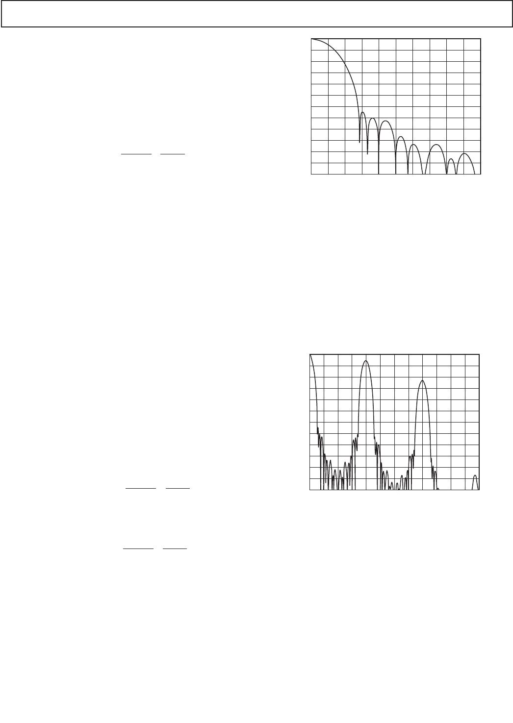
no overshoot.
Figure 11 shows the full frequency response of the AD7730 when
the second stage filter is set for normal FIR operation. This
response is for chop mode enabled with the decimal equivalent
of the word in the SF bits set to 512 and a master clock frequency
of 4.9152 MHz. The response will scale proportionately with
master clock frequency. The response is shown from dc to
100 Hz. The rejection at 50 Hz ±1 Hz and 60 Hz ± 1 Hz is
better than 88 dB.
The –3 dB frequency for the frequency response of the AD7730
with the second stage filter set for normal FIR operation and
chop mode enabled is determined by the following relationship:
f
3dB
= 0.0395 ×
f
CLK IN
16
×
1
3× SF
In this case, f
3 dB
= 7.9 Hz and the stopband, where the attenua-
tion is greater than 64.5 dB, is determined by:
f
STOP
= 0.14 ×
f
CLK IN
16
×
1
3× SF
In this case, f
STOP
= 28 Hz.
FREQUENCY – Hz
0
–60
–100
090
GAIN – dB
10 20 30 40 50 60 70 80
–10
–50
–70
–90
–30
–40
–80
–20
–120
–110
100
Figure 11. Detailed Full Frequency Response of AD7730
(Second Stage Filter as Normal FIR, Chop Enabled)
Figure 12 shows the frequency response for the same set of
conditions as for Figure 11, but in this case the response is
shown out to 600 Hz. This response shows that the attenuation
of input frequencies close to 200 Hz and 400 Hz is significantly
less than at other input frequencies. These “peaks” in the fre-
quency response are a by-product of the chopping of the input.
The plot of Figure 12 is the amplitude for different input fre-
quencies. Note that because the output rate is 200 Hz for the
conditions under which Figure 12 is plotted, if something ex-
isted in the input frequency domain at 200 Hz, it would be
aliased and appear in the output frequency domain at dc.
FREQUENCY – Hz
0
–60
–100
0 450
GAIN – dB
50 100 150 200 250 300 350 400
–10
–50
–70
–90
–30
–40
–80
–20
–120
–110
500 550 600
Figure 12. Expanded Full Frequency Response of AD7730
(Second Stage Filter as Normal FIR, Chop Enabled)
REV. B

AD7730LBRUZ-REEL7

Mfr. #:
Manufacturer:
Analog Devices Inc.
Description:
Analog to Digital Converters - ADC CMOS 24-Bit Low Pwr
Lifecycle:
New from this manufacturer.
Delivery:
DHL FedEx Ups TNT EMS
Payment:
T/T Paypal Visa MoneyGram Western Union