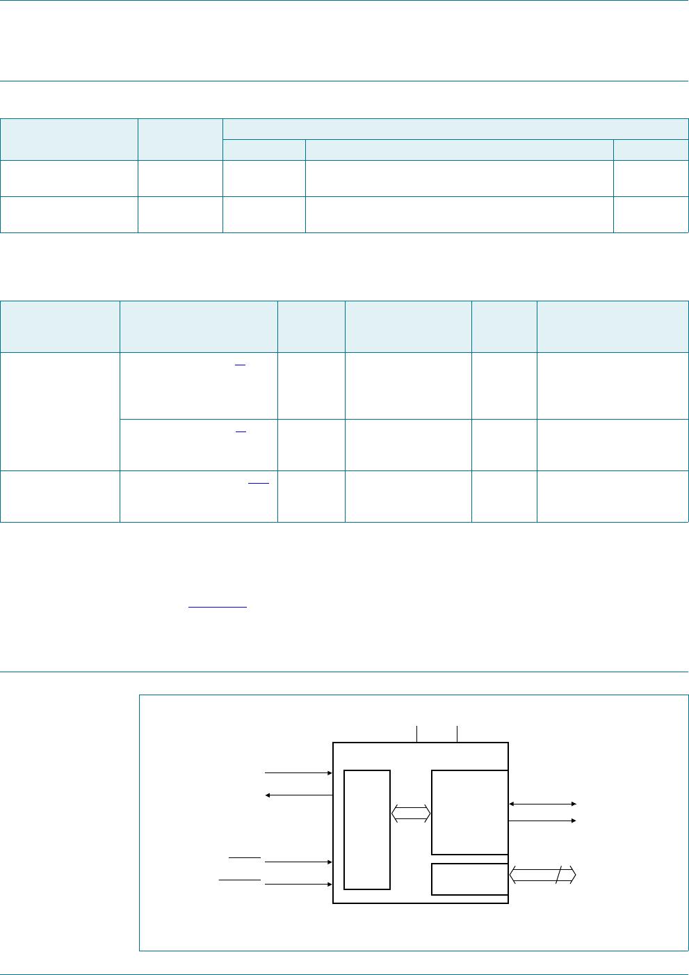
1. General description
The SC18IM700 is designed to serve as an interface between the standard UART port of
a microcontroller or microprocessor and the serial I
2
C-bus; this allows the microcontroller
or microprocessor to communicate directly with other I
2
C-bus devices. The SC18IM700
can operate as an I
2
C-bus master. The SC18IM700 controls all the I
2
C-bus specific
sequences, protocol, arbitration and timing. The host communicates with SC18IM700 with
ASCII messages protocol; this makes the control sequences from the host to the
SC18IM700 become very simple.
2. Features and benefits
UART host interface
I
2
C-bus controller
Eight programmable I/O pins
High-speed UART: baud rate up to 460.8 kbit/s
High-speed I
2
C-bus: 400 kbit/s
16-byte TX FIFO
16-byte RX FIFO
Programmable baud rate generator
2.4 V and 3.6 V operation
Sleep mode (power-down)
UART message format resembles I
2
C-bus transaction format
I
2
C-bus master functions
Multi-master capability
5 V tolerance on the input pins
8 N 1 UART format (8 data bits, no parity bit, 1 stop bit)
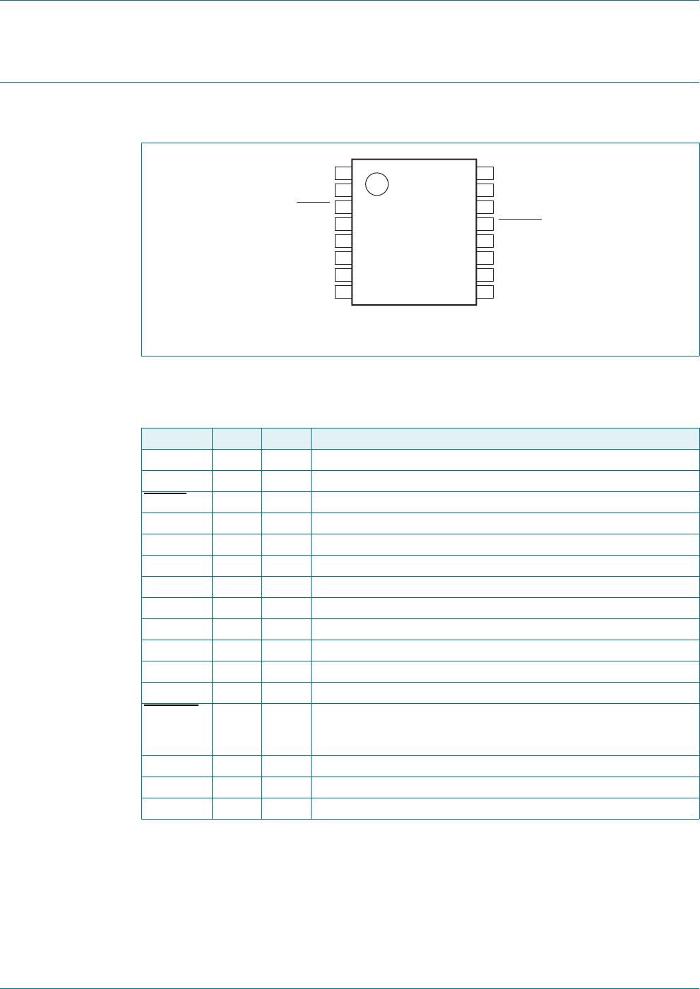
Available in very small TSSOP16 package
3. Applications
Enable I
2
C-bus master support in a system
I
2
C-bus instrumentation and control
Industrial control
Medical equipment
Cellular telephones
Handheld computers
SC18IM700
Master I
2
C-bus controller with UART interface
Rev. 3 — 12 October 2017 Product data sheet
SC18IM700_3 All information provided in this document is subject to legal disclaimers. © NXP Semiconductors N.V. 2017. All rights reserved.
Product data sheet Rev. 3 — 12 October 2017 2 of 24
NXP Semiconductors
SC18IM700
Master I
2
C-bus controller with UART interface
4. Ordering information
4.1 Ordering options
[1] Discontinued 201706009DN with Last Time Buy 12/7/2018 and Last Time Ship 6/6/2019.
[2] NXP plans to supply the /S8 device which is identical to the discontinued device for a minimum of 7 years with an expected
discontinuation in the 2024-2025 timeframe, but in the meantime, Failure Analysis for /S8 devices will consist of Automated Test
Equipment (ATE) and electrical overstress verification along with package and wire bond validation only. Detailed device failure analysis
will not be available; refer to CIN 201708035I
.
[3] The ",128" packing code for tape and reel with pin 1 in Q2 is now "HP".
5. Block diagram
Table 1. Ordering information
Type number Topside
marking
Package
Name Description Version
SC18IM700IPW IM700 B TSSOP16 plastic thin shrink small outline package; 16 leads;
body width 4.4 mm
SOT403-1
SC18IM700IPW/S8 IM700 B TSSOP16 plastic thin shrink small outline package; 16 leads;
body width 4.4 mm
SOT403-1
Table 2. Ordering options
Type number Orderable part number Package Packing method Minimum
order
quantity
Temperature
SC18IM700IPW SC18IM700IPW,112
[1]
TSSOP16 STANDARD
MARKING * IC'S
TUBE - DSC BULK
PACK
2400 T
amb
= 40 C to +85 C
SC18IM700IPW,128
[1]
TSSOP16 REEL 13" Q2/T3
*STANDARD MARK
SMD
2500 T
amb
= 40 C to +85 C
SC18IM700IPW/S8 SC18IM700IPW/S8HP
[2][3]
TSSOP16 REEL 13" Q2/T3
*STANDARD MARK
SMD
2500 T
amb
= 40 C to +85 C
Fig 1. Block diagram of SC18IM700
SC18IM700
I
2
C-BUS
CONTROLLER
002aab743
V
DD
UART
SCL
SDA
GPIO
REGISTER
GPIOs
RX
TX
WAKEUP
8
RESET
V
SS
SC18IM700_3 All information provided in this document is subject to legal disclaimers. © NXP Semiconductors N.V. 2017. All rights reserved.
Product data sheet Rev. 3 — 12 October 2017 3 of 24
NXP Semiconductors
SC18IM700
Master I
2
C-bus controller with UART interface
6. Pinning information
6.1 Pinning
6.2 Pin description
Fig 2. Pin configuration for TSSOP16
SC18IM700IPW
SC18IM700IPW/S8
GPIO0 GPIO7
GPIO1 GPIO4
RESET GPIO5
V
SS
WAKEUP
GPIO2 V
DD
GPIO3 GPIO6
SDA TX
SCL RX
002aab798
1
2
3
4
5
6
7
8
10
9
12
11
14
13
16
15
Table 3. Pin description
Symbol Pin Type Description
GPIO0 1 I/O programmable I/O pin
GPIO1 2 I/O programmable I/O pin
RESET
3 I hardware reset input
V
SS
4 - ground
GPIO2 5 I/O programmable I/O pin
GPIO3 6 I/O programmable I/O pin
SDA 7 I/O I
2
C-bus data pin
SCL 8 O I
2
C-bus clock output
RX 9 I RS-232 receive input
TX 10 O RS-232 transmit input
GPIO6 11 I/O programmable I/O pin
V
DD
12 - power supply
WAKEUP
13 I Wake up SC18IM700 from Power-down mode. Pulling LOW by the
host to wake up the device. A 1 k resistor must be connected
between V
DD
and this pin.
GPIO5 14 I/O programmable I/O pin
GPIO4 15 O programmable I/O pin
GPIO7 16 O programmable I/O pin

SC18IM700IPW/S8HP

Mfr. #:
Manufacturer:
NXP Semiconductors
Description:
I/O Controller Interface IC Master I2C-bus Controller w/UART
Lifecycle:
New from this manufacturer.
Delivery:
DHL FedEx Ups TNT EMS
Payment:
T/T Paypal Visa MoneyGram Western Union

Products related to this Datasheet