SC18IM700_3 All information provided in this document is subject to legal disclaimers. © NXP Semiconductors N.V. 2017. All rights reserved.
Product data sheet Rev. 3 — 12 October 2017 7 of 24
NXP Semiconductors
SC18IM700
Master I
2
C-bus controller with UART interface
7.1.8 Repeated START: write after write
The SC18IM700 also supports ‘write after write’ command as specified in the NXP
Semiconductors I
2
C-bus specification. This allows a write command to be sent after a
write command without having to issue a STOP condition between the two commands.
The host issues a write command as normal, then immediately issues a second write
command without sending a STOP (P) character after the first write command.
7.1.9 Power-down mode
The SC18IM700 can be placed in a low-power mode. In this mode the internal oscillator is
stopped and SC18IM700 will no longer respond to the host messages. Enter the
Power-down mode by sending the power-down character Z (0x5A) followed by the two
defined bytes, which are 0x5A and followed by 0xA5. If the exact message is not received,
the device will not enter the power-down state.
Upon entering the power-down state, SC18IM700 places the WAKEUP
pin in a HIGH
state. To have the device leave the power-down state, the WAKEUP
pin should be
brought LOW. A 1 k resistor must be connected between the WAKEUP
pin and V
DD
.
Fig 9. Repeated START: read after write
Fig 10. Repeated START: write after write
002aac055
NUMBER
OF BYTES
S CHAR.
SLAVE ADR.
+ W
S CHAR.
NUMBER
OF BYTES
SLAVE ADR. + W DATA 0
DATA 0
DATA N
P CHAR.DATA N
Fig 11. Power-down mode
002aac056
Z CHAR. 0x5A 0xA5 P CHAR.
SC18IM700_3 All information provided in this document is subject to legal disclaimers. © NXP Semiconductors N.V. 2017. All rights reserved.
Product data sheet Rev. 3 — 12 October 2017 8 of 24
NXP Semiconductors
SC18IM700
Master I
2
C-bus controller with UART interface
8. I
2
C-bus serial interface
The I
2
C-bus uses two wires (SDA and SCL) to transfer information between devices
connected to the bus, and it has the following features:
Bidirectional data transfer between masters and slaves
Multi-master bus (no central master)
Arbitration between simultaneously transmitting masters without corruption of serial
data on the bus
Serial clock synchronization allows devices with different bit rates to communicate via
one serial bus
Serial clock synchronization can be used as a handshake mechanism to suspend and
resume serial transfer.
A typical I
2
C-bus configuration is shown in Figure 12. The SC18IM700 device provides a
byte-oriented I
2
C-bus interface that supports data transfers up to 400 kHz.
Fig 12. I
2
C-bus configuration
R
PU
002aab801
V
DD
SC18IM700
I
2
C-BUS
DEVICE
I
2
C-BUS
DEVICE
I
2
C-bus
SDA
SCL
R
PU
xxxxxxxxxxxxxxxxxxxxx xxxxxxxxxxxxxxxxxxxxxxxxxx xxxxxxx x x x xxxxxxxxxxxxxxxxxxxxxxxxxxxxxx xxxxxxxxxxxxxxxxxxx xx xx xxxxx
xxxxxxxxxxxxxxxxxxxxxxxxxxx xxxxxxxxxxxxxxxxxxx xxxxxx xxxxxxxxxxxxxxxxxxxxxxxxxxxxxxxxxxx xxxxxxxxxxxx x x
xxxxxxxxxxxxxxxxxxxxx xxxxxxxxxxxxxxxxxxxxxxxxxxxxxx xxxxx xxxxxxxxxxxxxxxxxxxxxxxxxxxxxxxxxxxxxxxxxxxxxxxxxx xxxxxxxx
xxxxxxxxxxxxxxxxxxxxxxxxx xxxxxxxxxxxxxxxxxxxx xxx
SC18IM700_3 All information provided in this document is subject to legal disclaimers. © NXP Semiconductors N.V. 2017. All rights reserved.
Product data sheet Rev. 3 — 12 October 2017 9 of 24
NXP Semiconductors
SC18IM700
Master I
2
C-bus controller with UART interface
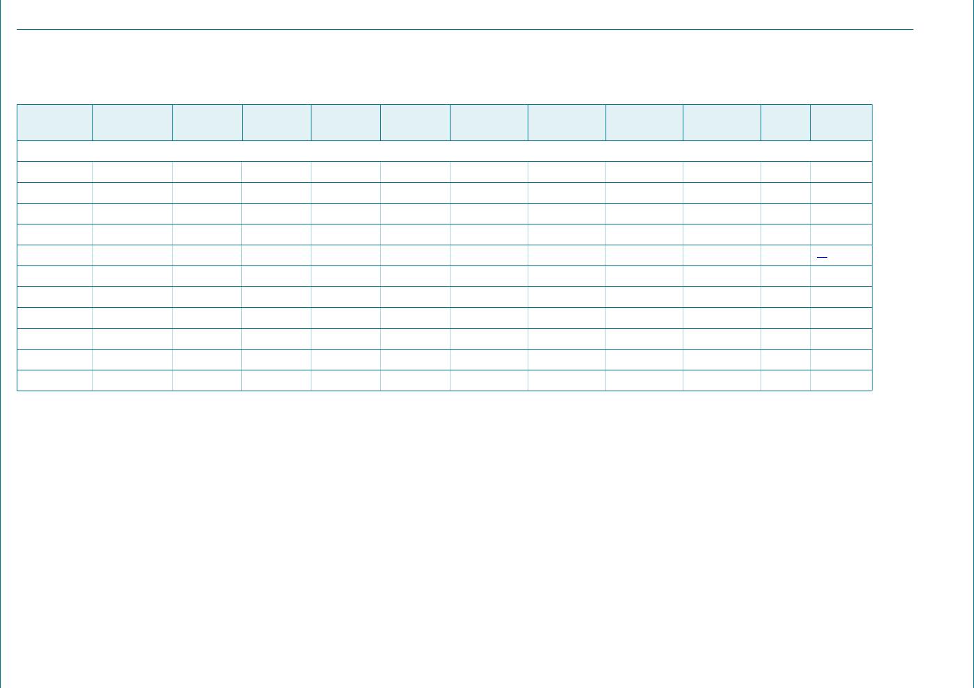
9. Internal registers available
9.1 Register summary
[1] Since the GPIO pins are configured as inputs after reset, the default value of this register depends on the states of the GPIO pins.
Table 5. Internal registers summary
Register
address
Register Bit 7 Bit 6 Bit 5 Bit 4 Bit 3 Bit 2 Bit 1 Bit 0 R/W Default
value
General register set
0x00 BRG0 bit 7 bit 6 bit 5 bit 4 bit 3 bit 2 bit 1 bit 0 R/W 0xF0
0x01 BRG1 bit 7 bit 6 bit 5 bit 4 bit 3 bit 2 bit 1 bit 0 R/W 0x02
0x02 PortConf1 GPIO3.1 GPIO3.0 GPIO2.1 GPIO2.0 GPIO1.1 GPIO1.0 GPIO0.1 GPIO0.0 R/W 0x55
0x03 PortConf2 GPIO7.1 GPIO7.0 GPIO6.1 GPIO6.0 GPIO5.1 GPIO5.0 GPIO4.1 GPIO4.0 R/W 0x55
0x04 IOState GPIO7 GPIO6 GPIO5 GPIO4 GPIO3 GPIO2 GPIO1 GPIO0 R/W -
[1]
0x05 reserved bit 7 bit 6 bit 5 bit 4 bit 3 bit 2 bit 1 bit 0 - 0x00
0x06 I2CAdr bit 7 bit 6 bit 5 bit 4 bit 3 bit 2 bit 1 bit 0 R/W 0x26
0x07 I2CClkL bit 7 bit 6 bit 5 bit 4 bit 3 bit 2 bit 1 bit 0 R/W 0x13
0x08 I2CClkH bit 7 bit 6 bit 5 bit 4 bit 3 bit 2 bit 1 bit 0 R/W 0x13
0x09 I2CTO TO7 TO6 TO5 TO4 TO3 TO2 TO1 TE R/W 0x66
0x0AI2CStat1111I2CStat[3]I2CStat[2]I2CStat[1]I2CStat[0]R0xF0

SC18IM700IPW/S8HP

Mfr. #:
Manufacturer:
NXP Semiconductors
Description:
I/O Controller Interface IC Master I2C-bus Controller w/UART
Lifecycle:
New from this manufacturer.
Delivery:
DHL FedEx Ups TNT EMS
Payment:
T/T Paypal Visa MoneyGram Western Union

Products related to this Datasheet