SC18IM700_3 All information provided in this document is subject to legal disclaimers. © NXP Semiconductors N.V. 2017. All rights reserved.
Product data sheet Rev. 3 — 12 October 2017 15 of 24
NXP Semiconductors
SC18IM700
Master I
2
C-bus controller with UART interface
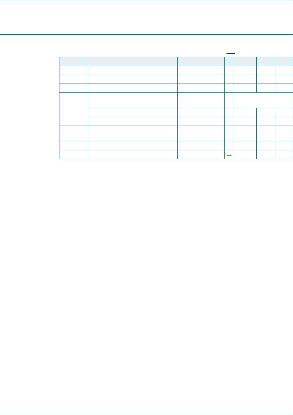
11. Static characteristics
[1] Typical ratings are not guaranteed. The values listed are at room temperature, 3 V.
[2] See Table 11 “
Limiting values” for steady state (non-transient) limits on I
OL
or I
OH
. If I
OL
/I
OH
exceeds the test condition, V
OL
/V
OH
may
exceed the related specification.
[3] Pin capacitance is characterized but not tested.
[4] Measured with GPIO in quasi-bidirectional mode.
[5] Measured with GPIO in high-impedance mode.
[6] GPIO in quasi-bidirectional mode with weak pull-up (applies to all GPIO pins with pull-ups). Does not apply to open-drain pins.
[7] GPIO pins source a transition current when used in quasi-bidirectional mode and externally driven from logic 1 to logic 0. This current is
highest when V
I
is approximately 2 V.
Table 12. Static characteristics
V
DD
= 2.4 V to 3.6 V; T
amb
=
40
Cto+85
C; unless otherwise specified.
Symbol Parameter Conditions Min Typ
[1]
Max Unit
I
DD
supply current V
DD
=3.6V
Operating mode; f = 7.3728 MHz - 9 15 mA
Idle mode; f = 7.3728 MHz - 3.25 5 mA
Power-down mode (sleep);
GPIO0 to GPIO7 as inputs;
inputs at V
DD
-5070A
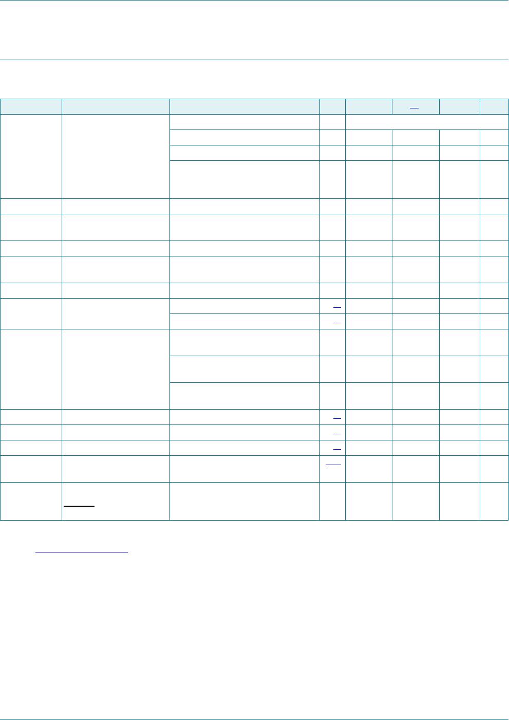
V
POR
power-on reset voltage - - 0.2 V
V
th(HL)
negative-going threshold
voltage
except SCL, SDA 0.22V
DD
0.4V
DD
-V
V
IL
LOW-level input voltage SCL, SDA only 0.5 - 0.3V
DD
V
V
th(LH)
positive-going threshold
voltage
except SCL, SDA - 0.6V
DD
0.7V
DD
V
V
IH
HIGH-level input voltage SCL, SDA only 0.7V
DD
-5.5V
V
OL
LOW-level output
voltage
I
OL
=20mA
[2]
-0.61.0V
I
OL
=3.2mA
[2]
-0.20.3V
V
OH
HIGH-level output
voltage
I
OH
= 20 mA; Push-pull mode;
GPIO3 to GPIO7
0.8V
DD
--V
I
OH
= 3.2 mA; Push-pull mode;
GPIO0toGPIO2
V
DD
0.7 V
DD
0.4 - V
I
OH
= 20 mA; quasi-bidirectional
mode; all GPIOs
V
DD
0.3 V
DD
0.2 - V
C
io
input/output capacitance
[3]
- - 15 pF
I
IL
LOW-level input current logic 0; all ports; V
I
=0.4V
[4]
--80 A
I
LI
input leakage current all ports; V
I
=V
IL
or V
IH
[5]
--10 A
I
T(HL)
negative-going transition
current
logic 1-to-0; all ports; V
I
=2.0V at
V
DD
=3.6V
[6][7]
30 - 450 A
R
RESET_N(int)
internal pull-up
resistance on pin
RESET
10 - 30 k