SC18IM700_3 All information provided in this document is subject to legal disclaimers. © NXP Semiconductors N.V. 2017. All rights reserved.
Product data sheet Rev. 3 — 12 October 2017 10 of 24
NXP Semiconductors
SC18IM700
Master I
2
C-bus controller with UART interface
9.2 Register descriptions
9.2.1 Baud Rate Generator (BRG)
The baud rate generator is an 8-bit counter that generates the data rate for the transmitter
and the receiver. The rate is programmed through the BRG register and the baud rate can
be calculated as follows:
(1)
Remark: To calculate the baud rate the values in the BRG registers must first be
converted from hex to decimal.
Remark: For the new baud rate to take effect, both BRG0 and BRG1 must be written in
sequence (BRG0, BRG1) with new values. The new baud rate will be in effect once BRG1
is written.
9.2.2 Programmable port configuration (PortConf1 and PortConf2)
GPIO port 0 to port 7 may be configured by software to one of four types. These are:
quasi-bidirectional, push-pull, open-drain, and input-only. Two bits are used to select the
desired configuration for each port pin. PortConf1 is used to select the configuration for
GPIO3 to GPIO0, and PortConf2 is used to select the configuration for GPIO7 to GPIO4.
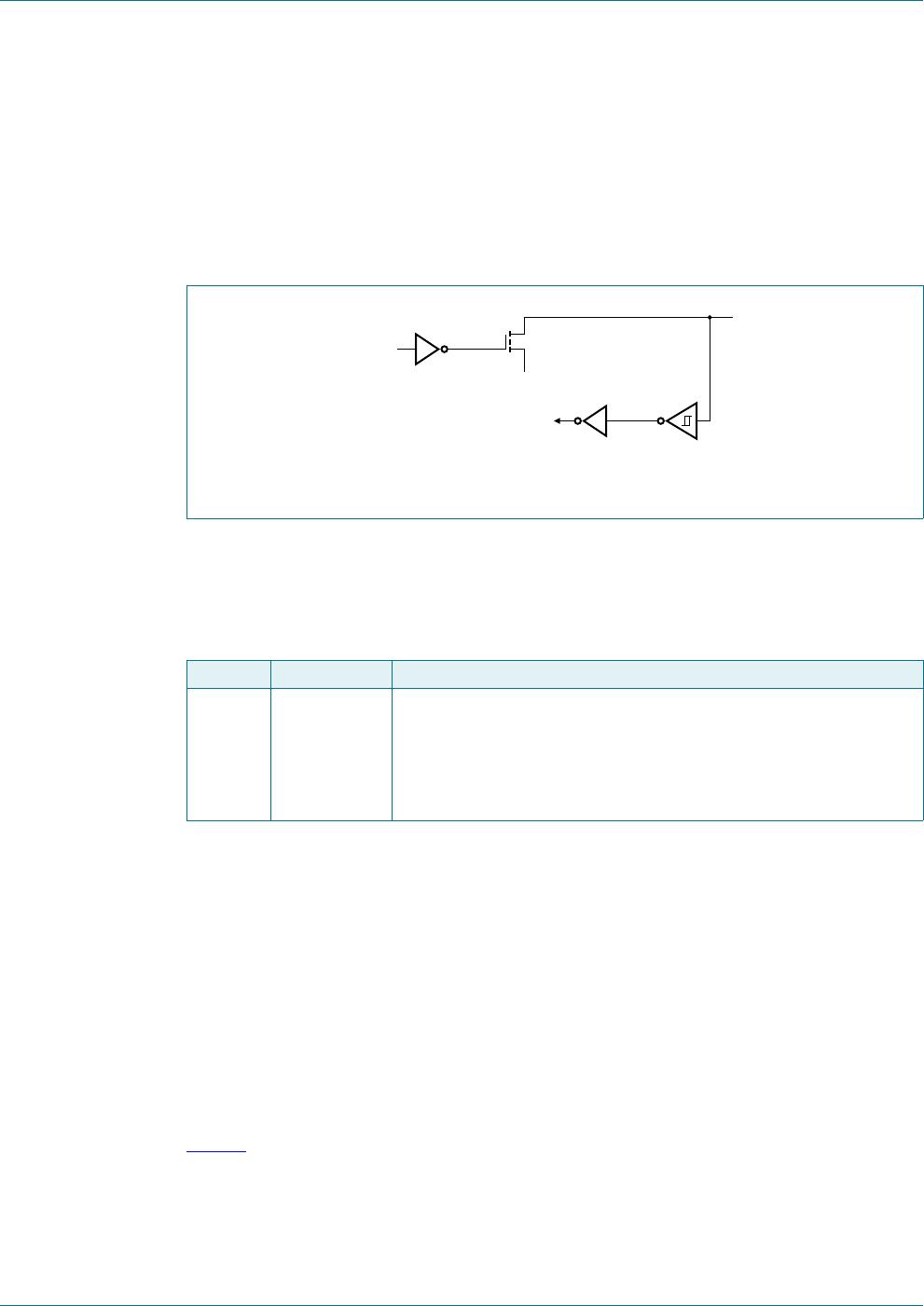
A port pin has Schmitt triggered input that also has a glitch suppression circuit.
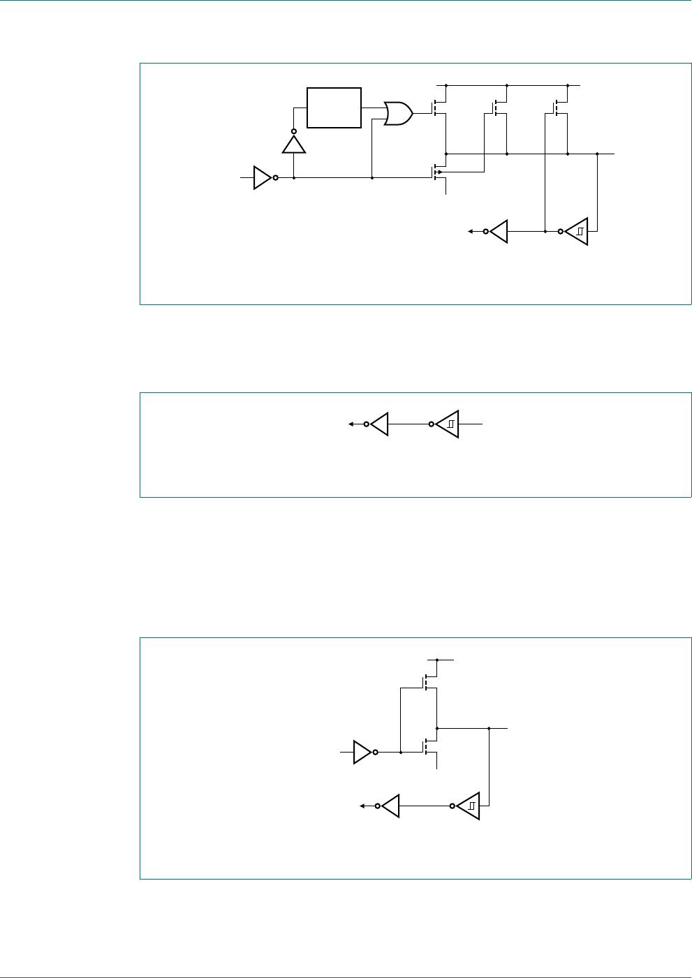
9.2.2.1 Quasi-bidirectional output configuration
Quasi-bidirectional output type can be used as both an input and output without the need
to reconfigure the port. This is possible because when the port outputs a logic HIGH, it is
weakly driven, allowing an external device to pull the pin LOW. When the pin is driven
LOW, it is driven strongly and able to sink a fairly large current. These features are
somewhat similar to an open-drain output except that there are three pull-up transistors in
the quasi-bidirectional output that serve different purposes.
The SC18IM700 is a 3 V device, but the pins are 5 V tolerant. In quasi-bidirectional mode,
if a user applies 5 V on the pin, there will be a current flowing from the pin to V
DD
, causing
extra power consumption. Therefore, applying 5 V in quasi-bidirectional mode is
discouraged.
A quasi-bidirectional port pin has a Schmitt triggered input that also has a glitch
suppression circuit.
Baud rate
7.3728 10
6
16 BRG1 BRG0+
-----------------------------------------------------
=
Table 6. Port configurations
GPIOx.1 GPIOx.0 Port configuration
0 0 quasi-bidirectional output configuration
0 1 input-only configuration
1 0 push-pull output configuration
1 1 open-drain output configuration
SC18IM700_3 All information provided in this document is subject to legal disclaimers. © NXP Semiconductors N.V. 2017. All rights reserved.
Product data sheet Rev. 3 — 12 October 2017 11 of 24
NXP Semiconductors
SC18IM700
Master I
2
C-bus controller with UART interface
9.2.2.2 Input-only configuration
The input-only port configuration has no output drivers. It is a Schmitt triggered input that
also has a glitch suppression circuit.
9.2.2.3 Push-pull output configuration
The push-pull output configuration has the same pull-down structure as both the
open-drain and the quasi-bidirectional output modes, but provides a continuous strong
pull-up when the port latch contains a logic 1. The push-pull mode may be used when
more source current is needed from a port output. A push-pull port pin has a Schmitt
triggered input that also has a glitch suppression circuit.
Fig 13. Quasi-bidirectional output configuration
002aac076
2 SYSTEM
CLOCK
CYCLES
weakstrong
very
weak
V
DD
PPP
V
SS
pin latch data
GPIOn
glitch rejection
input data
Fig 14. Input-only configuration
002aab884
GPIO pin
glitch rejection
input data
Fig 15. Push-pull output configuration
002aab885
strong
V
DD
P
V
SS
pin latch data
GPIO pin
glitch rejection
input data
N
SC18IM700_3 All information provided in this document is subject to legal disclaimers. © NXP Semiconductors N.V. 2017. All rights reserved.
Product data sheet Rev. 3 — 12 October 2017 12 of 24
NXP Semiconductors
SC18IM700
Master I
2
C-bus controller with UART interface
9.2.2.4 Open-drain output configuration
The open-drain output configuration turns off all pull-ups and only drives the pull-down
transistor of the port driver when the port latch contains a logic 0. To be used as a logic
output, a port configured in this manner must have an external pull-up, typically a resistor
tied to V
DD
.
An open-drain port pin has a Schmitt triggered input that also has a glitch suppression
circuit.
9.2.3 Programmable I/O pins state register (IOState)
When read, this register returns the actual state of all I/O pins. When written, each register
bit will be transferred to the corresponding I/O pin programmed as output.
9.2.4 I
2
C-bus address register (I2CAdr)
The contents of the register represents the device’s own I
2
C-bus address. The most
significant bit corresponds to the first bit received from the I
2
C-bus after a START
condition. A logic 1 in I2CAdr corresponds to a HIGH level on the I
2
C-bus, and a logic 0
corresponds to a LOW level on the I
2
C-bus. The least significant bit is not used, but
should be programmed with a ‘0’.
I2CAdr is not needed for device operation, but should be configured so that its address
does not conflict with an I
2
C-bus device address used by the bus master.
9.2.5 I
2
C-bus clock rates (I2CClk)
This register determines the serial clock frequency. The various serial rates are shown in
Table 8
. The frequency can be determined using the following formula:
(2)
I2CClkH determines the SCL HIGH period, and I2CClkL determines the SCL LOW period.
Fig 16. Open-drain output configuration
002aab883
V
SS
pin latch data
GPIO pin
glitch rejection
input data
Table 7. IOState - Programmable I/O pins state register (address 0x04h) bit description
Bit Symbol Description
7:0 IOLevel Set the logic level on the output pins.
Write to this register:
logic 0 = set output pin to zero
logic 1 = set output pin to one
Read this register returns states of all pins.
bit frequency
7.3728 10
6
2 I2CClkH I2CClkL+
-------------------------------------------------------------------
=

SC18IM700IPW/S8HP

Mfr. #:
Manufacturer:
NXP Semiconductors
Description:
I/O Controller Interface IC Master I2C-bus Controller w/UART
Lifecycle:
New from this manufacturer.
Delivery:
DHL FedEx Ups TNT EMS
Payment:
T/T Paypal Visa MoneyGram Western Union

Products related to this Datasheet