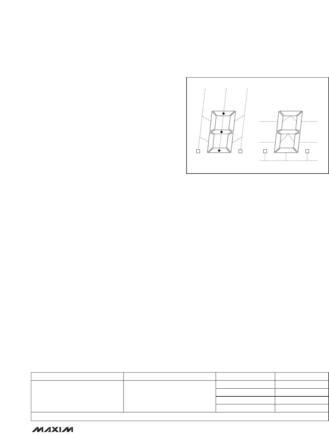
MAX1492/MAX1494
Detailed Description
The MAX1492/MAX1494 low-power, highly integrated
ADCs with LCD drivers convert a ±2V differential input
voltage (one count is equal to 100µV for the MAX1494
and 1mV for the MAX1492) with a sigma-delta ADC and
output the result to an LCD or µC. An additional
±200mV input range (one count is equal to 10µV for the
MAX1494 and 100µV for the MAX1492) is available to
measure small signals with increased resolution.
The devices operate from a single 2.7V to 5.25V power
supply and offer 3.5-digit (MAX1492) or 4.5-digit
(MAX1494) conversion results. An internal 2.048V refer-
ence, an internal charge pump, and a high-accuracy
on-chip oscillator eliminate external components.
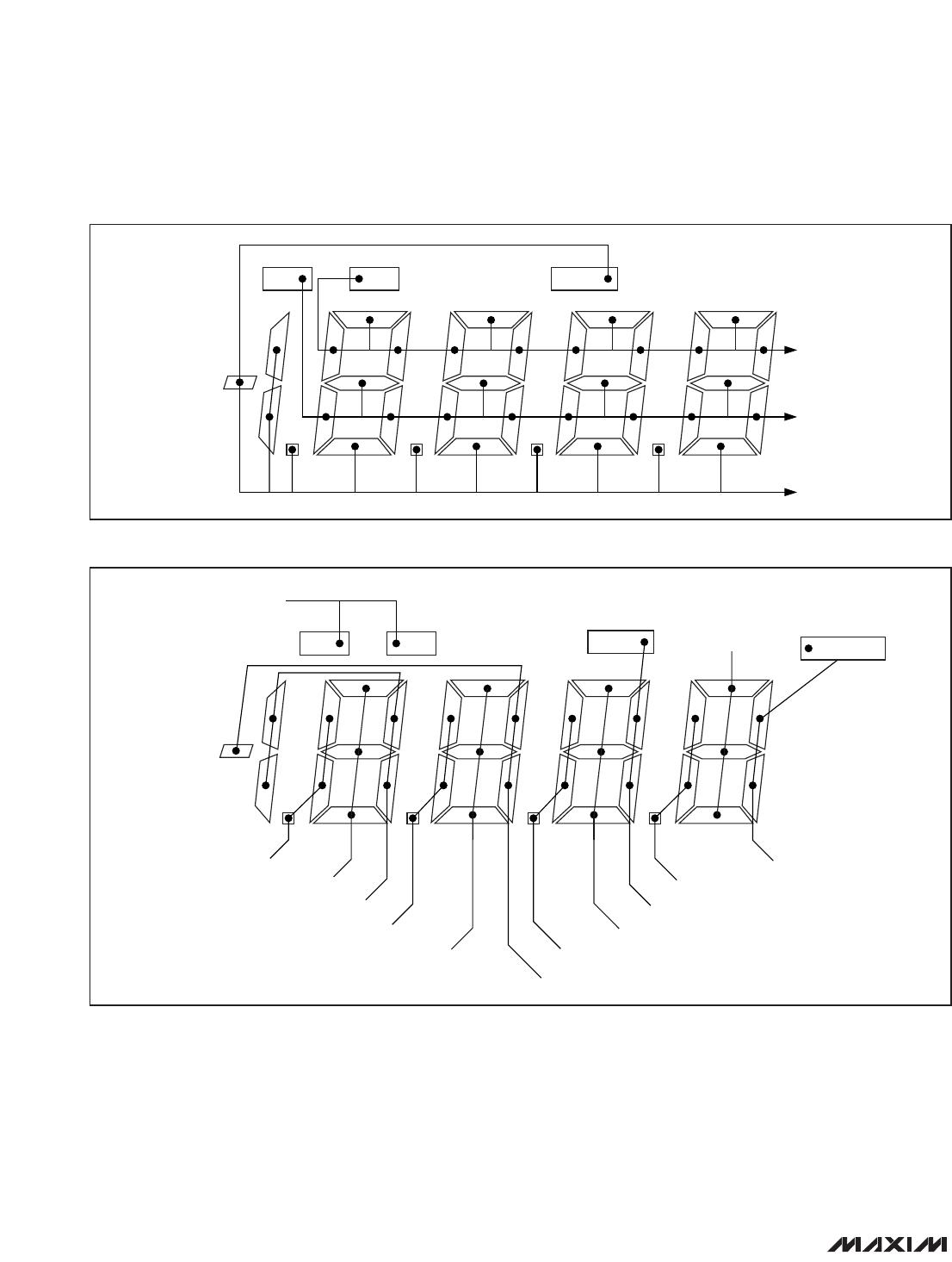
The MAX1492 and MAX1494 interface with a µC using
an SPI/QSPI/MICROWIRE-compatible serial interface.
Data can either be sent directly to the display or to the
µC first for processing before being displayed.
The devices also feature on-chip buffers for the differen-
tial input signal and external reference inputs, allowing
direct interface with high-impedance signal sources. In
addition, they use continuous internal-offset calibration
and offer >100dB of 50Hz and 60Hz line noise rejec-
tion. Other features include data hold and peak hold,
overrange and underrange detection, and a low-battery
monitor.
Analog Input Protection
Internal protection diodes limit the analog input range
from V
NEG
to (V
AVDD
+ 0.3V). If the analog input
exceeds this range, limit the input current to 10mA.
Internal Analog Input/Reference Buffers
The MAX1492/MAX1494 analog input/reference buffers
allow the use of high-impedance signal sources. The
input buffer’s common-mode input range allows the ana-
log inputs and the reference to range from -2.2V to +2.2V.
Modulator
The MAX1492/MAX1494 perform analog-to-digital con-
versions using a single-bit, 3rd-order, sigma-delta mod-
ulator. The sigma-delta modulator converts the input
signal into a digital pulse train whose average duty
cycle represents the digitized signal information. The
modulator quantizes the input signal at a much higher
sample rate than the bandwidth of the input.
The MAX1492/MAX1494 modulator provides 3rd-order
frequency shaping of the quantization noise resulting
from the single-bit quantizer. The modulator is fully dif-
ferential for maximum signal-to-noise ratio and mini-
mum susceptibility to power-supply noise. A single-bit
data stream is then presented to the digital filter to
remove the frequency-shaped quantization noise.
Digital Filtering
The MAX1492/MAX1494 contain an on-chip digital low-
pass filter that processes the data stream from the
modulator using a SINC
4
((sinx/x)
4
) response. The
SINC
4
filter has a settling time of four output data peri-
ods (4 x 200ms).
The MAX1492/MAX1494 have 25% overrange capability
built into the modulator and digital filter.
The digital filter is optimized for f
CLK
equal to 4.9152MHz.
Lower clock frequencies can be used; however,
50Hz/60Hz noise rejection decreases. The frequency
response of the SINC
4
filter is measured as follows:
where N is the oversampling ratio, and fm = N
output
data rate = 5Hz.
Filter Characteristics
Figure 2 shows the filter frequency response. The
SINC
4
characteristic -3dB cutoff frequency is 0.228
times the first-notch frequency (5Hz).
The output data rate for the digital filter corresponds
with the positioning of the first notch of the filter’s fre-
quency response. The notches of the SINC
4
filter are
repeated at multiples of the first-notch frequency. The
SINC
4
filter provides an attenuation of better than
100dB at these notches. For example, 50Hz is equal to
Hz
N
z
z
Hf
N
N
f
fm
f
fm
N
()
()
()
()
sin
sin
=
=
11
1
1
1
4
4
π
π
3.5- and 4.5-Digit, Single-Chip ADCs
with LCD Drivers
10 ___________________________________________________________________________________________________
FREQUENCY (Hz)
GAIN (dB)
5040302010
-160
-120
-80
-40
0
-200
060
Figure 2. Frequency Response of the SINC
4
Filter (Notch at 60Hz)
ten times the first-notch frequency and 60Hz is equal to
12 times the first-notch frequency.
For large step changes at the input, allow a settling
time of 800ms before valid data is read.
Clock Modes
Configure the MAX1492/MAX1494 to use either the
internal oscillator or an externally applied clock to drive
the modulator and filter. Set the EXTCLK bit in the con-
trol register to 0 to put the device in internal clock mode.
Set the EXTCLK bit high to put the device in external
clock mode. Connect CLK to GND or DVDD when using
the internal oscillator. The MAX1492/MAX1494 ideally
operate with a 4.9152MHz clock to achieve maximum
rejection of 50Hz/60Hz common-mode, power-supply,
and normal-mode noise.
Internal Clock Mode
The MAX1492/MAX1494 contain an internal oscillator.
The power-up condition for the MAX1492/MAX1494 is
internal clock operation with the EXTCLK bit in the con-
trol register equal to 0. Using the internal oscillator
saves board space by removing the need for an exter-
nal clock source.
External Clock Mode
For external clock operation, set the EXTCLK bit in the
control register high and drive CLK with a 4.9152MHz
clock source. Using an external clock allows for custom
conversion rates. A 2.4576MHz clock signal reduces
the conversion rate and the LCD update rate by a fac-
tor of two. The MAX1492/MAX1494 operate with an
external clock source of up to 5.05MHz.
Charge Pump
The MAX1492/MAX1494 contain an internal charge
pump to provide the negative supply voltage for the inter-
nal analog input/reference buffers. The bipolar input
range of the analog input/reference buffers allows this
device to accept negative inputs with high source imped-
ances. Connect a 0.1µF capacitor from V
NEG
to GND.
LCD Driver
The MAX1492/MAX1494 contain the necessary back-
plane and segment-driver outputs to drive 3.5-digit
(MAX1492) and 4.5-digit (MAX1494) LCDs. The LCD
update rate is 2.5Hz. Figures 4–7 show the connection
schemes for a standard LCD. The MAX1492/MAX1494
automatically display the results of the ADC, if desired.
The MAX1492/MAX1494 also allow independent control
of the LCD driver through the serial interface, allowing
for data processing of the ADC result before showing
the result on the LCD. Additionally, each LCD segment
can be individually controlled (see the
LCD Segment-
Display Register
sections).
Triplexing
An internal resistor string comprised of three equal-
value resistors (52k, 1% matching) is used to gener-
ate the display drive voltages. On the MAX1492, one
end of the string is connected to DVDD and the other
end is connected to GND. On the MAX1494, the other
end of the resistor string is connected to V
DISP
. Note
that V
LCD
should be three times the threshold voltage
for the liquid crystal material used (Figure 9).
The connection diagrams for a typical 7-segment dis-
play-font decimal point and annunciators are illustrated
in Figures 3 and 8. The MAX1494/MAX1492 numeric
display drivers (4.5 digits, 3.5 digits) use this configura-
tion to drive a triplexed LCD with three backplanes and
13 segment-driver lines (10 for 3.5 digits). Figures 4
MAX1492/MAX1494
3.5- and 4.5-Digit, Single-Chip ADCs
with LCD Drivers
______________________________________________________________________________________ 11
a
XYZ
g
d
e
f
c
b
DP
ANNUNCIATOR
a
g
d
e
f
c
b
DP ANNUNCIATOR
BP1
BP2
BP3
Figure 3. Connection Diagrams for Typical 7-Segment Displays
MANUFACTURER WEBSITE PART NUMBER DESCRIPTION
04-0924-00 3.5 digits, 5V
04-0924-01 3.5 digits, 3V
04-0925-00 4.5 digits, 5V
DCI, Inc. www.dciincorporated.com
04-0925-01 4.5 digits, 3V
The following site has links to other custom LCD manufacturers: www.earthlcd.com/mfr.htm
Table 1. List of Custom LCD Manufacturers
MAX1492/MAX1494
and 5 show the assignment of the 4.5-digit display seg-
ments, and Figures 6 and 7 show the assignment of the
3.5-digit display segments.
The voltage waveforms of the backplane lines and Y
segment line (Figure 3) have been chosen as an exam-
ple. This line intersects with BP1 to form the a segment,
with BP2 to form the g segment, and with BP3 to form
the d segment. Eight different ON/OFF combinations of
the a, g, and d segments and their corresponding
waveforms of the Y segment line are illustrated in
Figures 9 and 10. The schematic diagram in Figure 8
shows each intersection as a capacitance from seg-
ment line to common line. Figure 11 illustrates the volt-
age across the g segment.
The RMS voltage across the segment determines the
degree of polarization for the liquid crystal material and
3.5- and 4.5-Digit, Single-Chip ADCs
with LCD Drivers
12 ______________________________________________________________________________________
HOLD LOW BATTPEAK
BP1
BP2
BP3
Figure 4. Backplane Connection for the MAX1494 (4.5 Digits)
HOLD
LOW BATT
PEAK
SEG13: PEAK, HOLD, N.C.
SEG2: A1, G1, D1
SEG12: F4, E4, DP4
SEG11: A4, G4, D4
SEG10: B4, C4, BC5
SEG9: F3, E3, DP3
SEG8: A3, G3, D3
SEG1: B1, C1, N.C.
SEG3: F1, E1, DP1
SEG4: B2, C2, LOWBATT
SEG5: A2, G2, D2
SEG6: F2, E2, DP2
SEG7: B3, C3, MINUS
ANNUNCIATOR
Figure 5. Segment Connection for the MAX1494 (4.5 Digits)

MAX1494CCJ+

Mfr. #:
Manufacturer:
Maxim Integrated
Description:
LCD Drivers 4.5 Digit ADC w/LCD Drivers
Lifecycle:
New from this manufacturer.
Delivery:
DHL FedEx Ups TNT EMS
Payment:
T/T Paypal Visa MoneyGram Western Union

Products related to this Datasheet