MAX1492/MAX1494
3.5- and 4.5-Digit, Single-Chip ADCs
with LCD Drivers
______________________________________________________________________________________ 21
Applications Information
Serial Interface
The SPI/QSPI/MICROWIRE serial interface consists of a
chip select (CS), a serial clock (SCLK), a data in (DIN),
a data out (DOUT), and an asynchronous EOC output.
EOC provides an asynchronous end-of-conversion sig-
nal with a period of 200ms (f
CLK
= 4.9152MHz or inter-
nal clock mode). The MAX1492 updates the data
register when EOC goes high. Data is valid in the ADC
result registers when EOC returns low. The serial inter-
face provides access to 12 on-chip registers, allowing
control to all the power modes and functional blocks.
Table 5 lists the address and read/write accessibility of
all the registers.
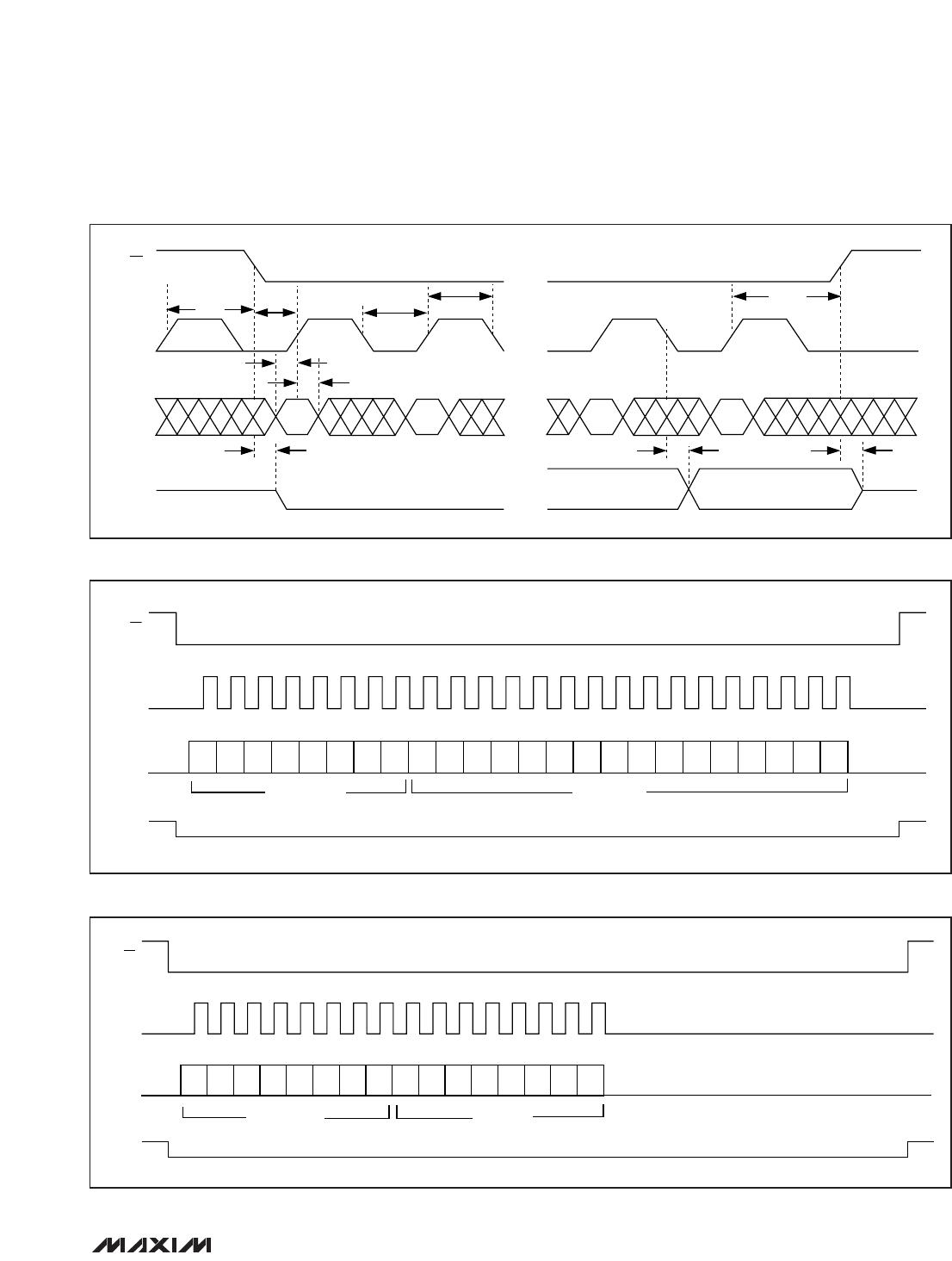
A logic-high on CS three-states DOUT and causes the
MAX1492/MAX1494 to ignore any signals on SCLK and
DIN. To clock data into or out of the internal shift regis-
ter, drive CS low. SCLK synchronizes the data transfer.
The rising edge of SCLK clocks DIN into the shift regis-
ter, and the falling edge of SCLK clocks DOUT out of
the shift register. DIN and DOUT are transferred MSB-
first (data is left justified). Figures 13–17 show the
detailed serial-interface timing diagrams for the 8- and
16-bit read/write operations.
All communication with the MAX1492/MAX1494 begins
with a command byte on DIN, where the first logic 1 on
DIN is recognized as the START bit (MSB) for the com-
mand byte. The following seven clock cycles load the
command into a shift register. These 7 bits specify
which of the registers are accessed next, and whether a
read or write operation takes place. Transitions on the
serial clock after the command byte transfer cause a
write or read from the device until the correct number of
bits have been transferred (8 or 16). Once this has
occurred, the MAX1492/MAX1494 wait for the next com-
mand byte. CS must not go high between data trans-
fers. If CS is toggled before the end of a write or read
operation, the device mode may be unknown. Clock in
32 zeros to clear the device state and reset the interface
so it is ready to receive a new command byte.
On-Chip Registers
The MAX1492/MAX1494 contain 12 on-chip registers.
These registers configure the various functions of the
device and allow independent reading of the ADC
results and writing to the LCD. Table 5 lists the address
and size of each register.
The first of these registers is the status register. The 8-bit
status register contains the status flags for the ADC. The
second register is the 16-bit control register. This register
sets the LCD controls, range modes, power-down
modes, offset calibration, and the reset-register function
(CLR). The third register is the 16-bit overrange register
that sets the overrange limit of the analog input. The
fourth register is the 16-bit underrange register that sets
the underrange limit of the analog input. Registers 5
through 7 contain the display data for the individual seg-
ments of the LCD. The eighth register contains the cus-
tom offset value. The ninth register contains the 16 MSBs
of the ADC conversion result. The tenth register contains
the LCD data. The eleventh register contains the peak
analog input value. The last register contains the lower 4
LSBs of the 20-bit ADC conversion result.