MAX1492/MAX1494
3.5- and 4.5-Digit, Single-Chip ADCs
with LCD Drivers
28 ______________________________________________________________________________________
Power-On Reset
At power-up, the serial interface, LCD driver, digital fil-
ter, and modulator circuits reset. The registers return to
their default values. Allow time for the reference to set-
tle before starting calibration.
Offset Calibration
The MAX1492/MAX1494 offer on-chip offset calibration.
The device offset-calibrates during every conversion
when the OFFSET_CAL1 bit is 0. Enhanced offset calibra-
tion is only needed in the MAX1494 when RANGE = 1.
It is performed on demand by setting the OFFSET_CAL2
bit to 1.
Power-Down Modes
The MAX1492/MAX1494 feature independent power-
down control of the analog and digital circuitry. Writing a
1 to the PD_DIG and PD_ANA bits in the control register
powers down the analog and digital circuitry, reducing
the supply current to 400µA. PD_DIG powers down the
digital filter and LCD drivers, while PD_ANA powers
down the analog modulator and ADC input buffers.
V
DISP
LCD Compensation (MAX1494 Only)
Adequate display contrast can be obtained in most
applications by connecting V
DISP
to GND. In applica-
tions where a wide temperature range is expected, the
voltage levels for some triplexed LCDs may need to vary
with temperature to maintain good display contrast and
viewing angle. The amount of temperature compensation
depends upon the type of liquid crystal used. Display
manufacturers usually specify the temperature variation
of the LCD thresholds voltage (RMS
ON
- RMS
OFF
), which
is approximately 1/3 of the peak display voltage. The
peak display voltage is equal to V
DVDD
- V
DISP
(MAX1494 only). Therefore, a typical -4mV/°C tempera-
ture coefficient of an LCD threshold corresponds to a
+12mV/°C temperature coefficient at V
DISP
.
Peak
The MAX1492/MAX1494 feature peak-detection circuit-
ry. When activated (PEAK bit = 1), the devices display
only the highest voltage measured to the LCD.
Hold
The MAX1492/MAX1494 feature data-hold circuitry.
When activated (HOLD bit = 1), the devices display the
current reading on the LCD.
Low Battery
The MAX1492/MAX1494 feature a low-battery detection
input. When the voltage at LOW BATT drops below
2.048V (typ), the LOW_BATT bit of the status register
goes high and the LOW BATT segment of the LCD turns
on.
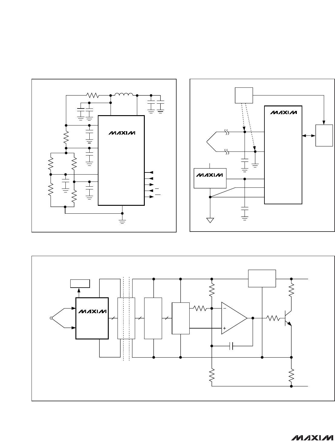
Strain Gauge Measurement
Connect the differential inputs of the MAX1492/
MAX1494 to the bridge network of the strain gauge. In
Figure 20, the analog supply voltage powers the bridge
network and the MAX1492/MAX1494 along with the ref-
erence voltage. The MAX1492/MAX1494 handle an
analog input-voltage range of ±200mV and ±2V full
scale. The analog/reference inputs of the parts allow
the analog input range to have an absolute value of
anywhere between -2.2V and +2.2V.
Thermocouple Measurement
Figure 21 shows a connection from a thermocouple to
the MAX1492/MAX1494. In this application, the
MAX1492/MAX1494 take advantage of the on-chip input
buffers that allow large source impedances on the front
end. The decoupling capacitors reduce noise pickup
from the thermocouple leads. To place the differential
voltage from the thermocouple at a suitable common-
mode voltage, the AIN- input of the MAX1492/MAX1494
is biased to GND. Use an external temperature sensor,
such as the DS75, and a µC to perform cold junction-
temperature compensation.
4–20mA Transmitter
Low-power, single-supply operations make the
MAX1492/MAX1494 ideal for loop-powered 4–20mA
transmitters. Loop-powered transmitters draw their
power from the 4–20mA loop, limiting the transmitter
circuitry to a current budget of 4mA. Tolerances in the
loop further limit this current budget to 3.5mA. Since
the MAX1492/MAX1494 only consume 950µA, a total of
2.55mA remains to power the remaining transmitter cir-
cuitry. Figure 22 shows a block diagram for a loop-
powered 4–20mA transmitter.
4–20mA Measurement
To measure 4–20mA signals, connect a shunt resistor
across AIN+ and AIN- to create the ±2V or ±200mV
input voltage (Figure 23).
Transfer Functions
Figures 24–27 show the transfer functions of the
MAX1492/MAX1494. The output data is stored in the
ADC data register in two’s complement.
A -1 in the ADC result register displays -0 on the LCD as
shown in Figures 24–27. Negative values on the LCD
are offset by 1. For example, -100 in the ADC result reg-
ister appears as -99 on the LCD.
Supplies, Layout, and Bypassing
When using analog and digital supplies from the same
source, isolate the digital supply from the analog sup-
ply with a low-value resistor (10Ω) or ferrite bead. For