MAX1492/MAX1494
3.5- and 4.5-Digit, Single-Chip ADCs
with LCD Drivers
______________________________________________________________________________________ 25
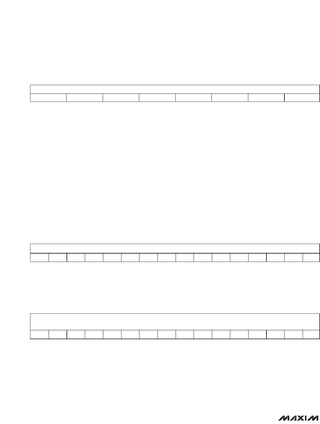
Default values: 0000h
The LCD segment-display register 2 is a 16-bit
read/write register. When the SEG_SEL bit (in the con-
trol register) is set to 1, the MAX1492/MAX1494 provide
direct access to individual LCD segments. The bits in
the LCD segment-display register determine if a seg-
ment is on or off. Write a 0 to this register to turn on a
segment and a 1 to turn off a segment.
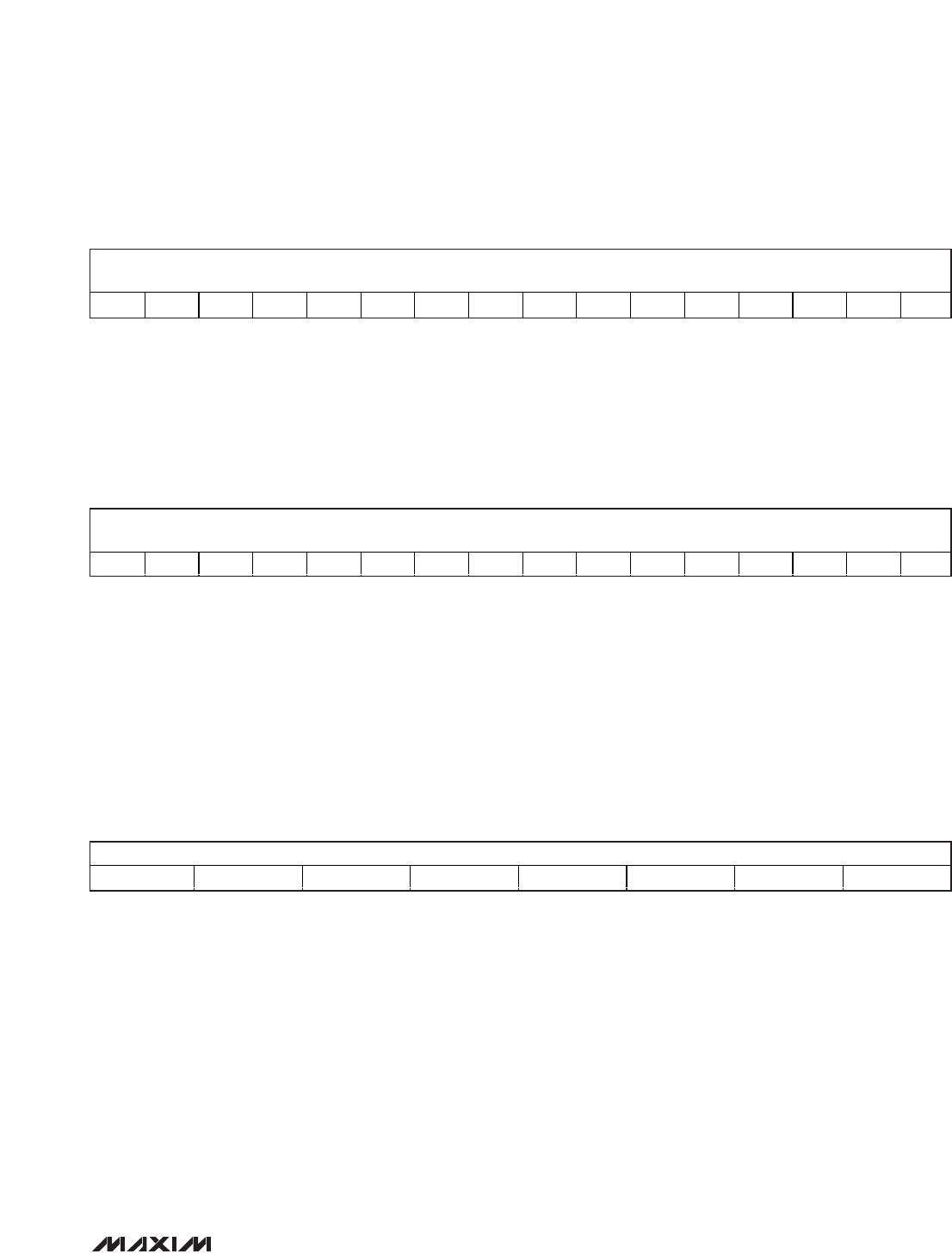
DP1: Segment DP Driver Bit of Digit 1. The
default value turns on the LCD segment.
E1: Segment e Driver Bit of Digit 1. The
default value turns on the LCD segment.
F1: Segment f Driver Bit of Digit 1. The
default value turns on the LCD segment.
D1: Segment d Driver Bit of Digit 1. The
default value turns on the LCD segment.
G1: Segment g Driver Bit of Digit 1. The
default value turns on the LCD segment.
A1: Segment a Driver Bit of Digit 1. The
default value turns on the LCD segment.
C1: Segment c Driver Bit of Digit 1. The
default value turns on the LCD segment.
B1: Segment b Driver Bit of Digit 1. The
default value turns on the LCD segment.
ANN: Custom Annunciator. The default value
turns on the LCD segment.
DP2: Segment DP Driver Bit of Digit 2. The
default value turns on the LCD segment.
E2: Segment e Driver Bit of Digit 2. The
default value turns on the LCD segment.
F2: Segment f Driver Bit of Digit 2. The
default value turns on the LCD segment.
D2: Segment d Driver Bit of Digit 2. The
default value turns on the LCD segment.
G2: Segment g Driver Bit of Digit 2. The
default value turns on the LCD segment.
A2: Segment a Driver Bit of Digit 2. The
default value turns on the LCD segment.
C2: Segment c Driver Bit of Digit 2. The
default value turns on the LCD segment.
B2: Segment b Driver Bit of Digit 2. The
default value turns on the LCD segment.
LOWBATT: LOWBATT Driver Bit. The default value
turns on the LOWBATT annunciator.
DP3: Segment DP Driver Bit of Digit 3. The
default value turns on the LCD segment.
E3: Segment e Driver Bit of Digit 3. The
default value turns on the LCD segment.
F3: Segment f Driver Bit of Digit 3. The
default value turns on the LCD segment.
D3: Segment d Driver Bit of Digit 3. The
default value turns on the LCD segment.
G3: Segment g Driver Bit of Digit 3. The
default value turns on the LCD segment.
A3: Segment a Driver Bit of Digit 3. The
default value turns on the LCD segment.
C3: Segment c Driver Bit of Digit 3. The
default value turns on the LCD segment.
B3: Segment b Driver Bit of Digit 3. The
default value turns on the LCD segment.
MINUS: Minus-Sign Driver Bit. The default value
turns on the LCD segment.
DP4: Segment DP Driver Bit of Digit 4. The
default value turns on the LCD segment
(MAX1494 only).
E4: Segment e Driver Bit of Digit 4. The
default value turns on the LCD segment
(MAX1494 only).
F4: Segment f Driver Bit of Digit 4. The
default value turns on the LCD segment
(MAX1494 only).
LCD Segment-Display Register 2 (Read/Write):