MAX1492/MAX1494
3.5- and 4.5-Digit, Single-Chip ADCs
with LCD Drivers
4 _______________________________________________________________________________________
ELECTRICAL CHARACTERISTICS (continued)
(V
AVDD
= V
DVDD
= 2.7V to 5.25V, V
GND
= 0V, V
REF+
- V
REF-
= 2.048V (external reference). Internal clock mode, unless otherwise noted.
All specifications are at T
A
= T
MIN
to T
MAX
, unless otherwise noted. Typical values are at T
A
= +25°C, unless otherwise noted.)
PARAMETER SYMBOL CONDITIONS MIN TYP MAX UNITS
CHARGE PUMP (C
NEG
= 0.1µF)
Output Voltage V
NEG
-2.60 -2.42 -2.30 V
DIGITAL INPUTS (SCLK, DIN, CS, CLK)
Input Current I
IN
V
IN
= 0V or V
DVDD
-10 +10 µA
Input Low Voltage V
INL
0.3 x
V
DVDD
V
Input High Voltage V
INH
0.7 x V
DVDD
V
Input Hysteresis V
HYST
V
DVDD
= 3.0V 200 mV
DIGITAL OUTPUTS (DOUT, EOC)
Output Low Voltage V
OL
I
SINK
= 1mA 0.4 V
Output High Voltage V
OH
I
SOURCE
= 200µA 0.8 x V
DVDD
V
Three-State Leakage Current I
L
DOUT only -10 +10 µA
Three-State Output Capacitance C
OUT
DOUT only 15 pF
POWER SUPPLY
AVDD Voltage V
AVDD
2.70 5.25 V
DVDD Voltage V
DVDD
2.70 5.25 V
Power-Supply Rejection AVDD PSRR
A
(Note 7) 80 dB
Power-Supply Rejection DVDD PSRR
D
(Note 7) 100 dB
V
AVDD
= 5V 580 660
AVDD Current (Notes 8, 9) I
AVDD
Standby 240 380
µA
V
DVDD
= 5V 260 320
V
DVDD
= 3.3V 130 180DVDD Current (Notes 8, 9) I
DVDD
Standby 10 20
µA
LCD DRIVER
MAX1492
1.92 x
V
DVDD
RMS Segment On Voltage
MAX1494
1.92 x
(V
DVDD
- V
DISP
)
V
MAX1492
1/3 x
V
DVDD
RMS Segment Off Voltage
MAX1494
1/3 x
(V
DVDD
- V
DISP
)
V
Display Voltage Setup Resistor R
DISP
MAX1494 only 157.5 k
Display Multiplex Rate 107 Hz
LCD Data-Update Rate 2.5 Hz
MAX1492/MAX1494
3.5- and 4.5-Digit, Single-Chip ADCs
with LCD Drivers
_______________________________________________________________________________________ 5
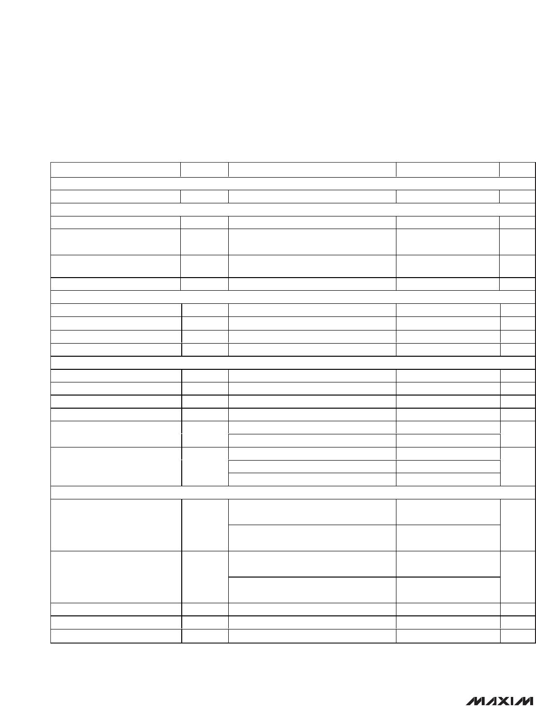
TIMING CHARACTERISTICS (Notes 10, 11 and Figure 13)
(V
AVDD
= V
DVDD
= 2.7V to 5.25V, V
GND
= 0V, T
A
= T
MIN
to T
MAX
, unless otherwise noted.)
PARAMETER SYMBOL CONDITIONS MIN TYP MAX UNITS
SCLK Operating Frequency f
SCLK
0 4.2 MHz
SCLK Pulse-Width High t
CH
100 ns
SCLK Pulse-Width Low t
CL
100 ns
DIN to SCLK Setup t
DS
50 ns
DIN to SCLK Hold t
DH
0ns
CS Fall to SCLK Rise Setup t
CSS
50 ns
SCLK Rise to CS Rise Hold t
CSH
0ns
SCLK Fall to DOUT Valid t
DO
C
LOAD
= 50pF (Figures 18, 19) 120 ns
CS Rise to DOUT Disable t
TR
C
LOAD
= 50pF (Figures 18, 19) 120 ns
CS Fall to DOUT Enable t
DV
C
LOAD
= 50pF (Figures 18, 19) 120 ns
Note 1: Integral nonlinearity is the deviation of the analog value at any code from its theoretical value after nulling the gain error
and offset error.
Note 2: Offset calibrated. See the
OFFSET_CAL1
and
OFFSET_CAL2
sections in the
On-Chip Registers
section.
Note 3: Offset nulled.
Note 4: Drift error is eliminated by recalibration at the new temperature.
Note 5: The input voltage range for the analog inputs is given with respect to the voltage on the negative input of the differential pair.
Note 6: V
AIN+
or V
AIN-
= -2.2V to +2.2V. V
REF+
or V
REF-
= -2.2V to +2.2V. All input structures are identical. Production tested on
AIN+ and REF+ only.
Note 7: Measured at DC by changing the power-supply voltage from 2.7V to 5.25V and measuring the effect on the conversion
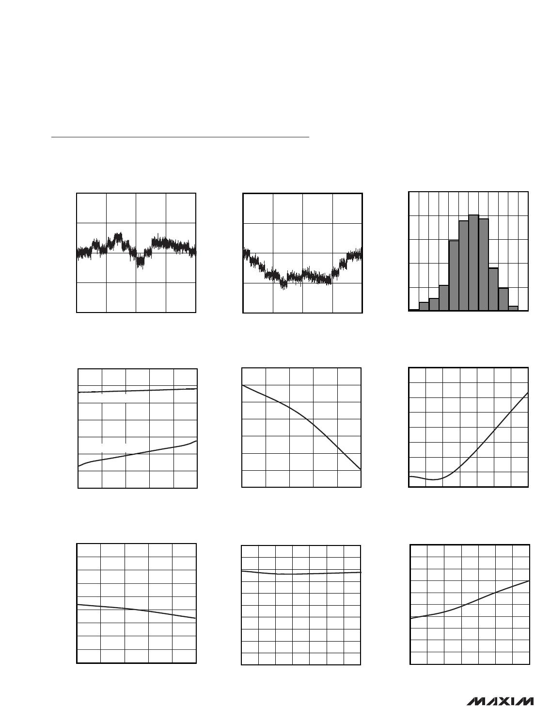
error with external reference. PSRR at 50Hz and 60Hz exceeds 120dB with filter notches at 50Hz and 60Hz (Figure 2).
Note 8: CLK and SCLK are idle.
Note 9: Power-supply currents are measured with all digital inputs at either GND or DVDD and with the device in internal clock mode.
Note 10: All input signals are specified with t
RISE
= t
FALL
= 5ns (10% to 90% of DVDD) and are timed from a voltage level of 50% of
DVDD, unless otherwise noted.
Note 11: See the serial-interface timing diagrams.
MAX1492/MAX1494
3.5- and 4.5-Digit, Single-Chip ADCs
with LCD Drivers
6 _______________________________________________________________________________________
Typical Operating Characteristics
(V
AVDD
= V
DVDD
= 5V, V
GND
= 0V, external reference mode, REF+ = 2.048V, REF- = GND, RANGE bit = 1, internal clock mode, T
A
=
+25°C, unless otherwise noted.)
MAX1494
(±200mV INPUT RANGE) INL vs. OUTPUT CODE
MAX1492/94 toc01
OUTPUT CODE
INL (COUNTS)
10,0000-10,000
-0.5
0
0.5
1.0
-1.0
-20,000 20,000
MAX1494
(±2V INPUT RANGE) INL vs. OUTPUT CODE
MAX1492/94 toc02
OUTPUT CODE
INL (COUNTS)
10,0000-10,000
-0.5
0
0.5
1.0
-1.0
-20,000 20,000
NOISE DISTRIBUTION
MAX1492/94 toc03
NOISE (LSB)
PERCENTAGE OF UNITS (%)
0.80.70.60.50.40.30.20.10-0.1
5
10
15
20
25
0
-0.2
SUPPLY CURRENT
vs. SUPPLY VOLTAGE
MAX1492/94 toc04
SUPPLY VOLTAGE (V)
SUPPLY CURRENT (µA)
4.754.253.753.25
100
200
300
400
500
600
700
0
2.75 5.25
ANALOG SUPPLY
DIGITAL SUPPLY
MAX1494
OFFSET ERROR vs. SUPPLY VOLTAGE
MAX1492/94 toc05
SUPPLY VOLTAGE (V)
OFFSET ERROR (LSB)
4.754.253.753.25
-0.11
-0.06
-0.01
0.04
0.09
0.14
0.19
-0.16
2.75 5.25
MAX1494
OFFSET ERROR vs. TEMPERATURE
MAX1492/94 toc06
TEMPERATURE (°C)
OFFSET ERROR (LSB)
605010 20 30 40
-0.1
0
0.1
0.2
0.3
0.4
0.5
0.6
-0.2
070
MAX1494
GAIN ERROR vs. SUPPLY VOLTAGE
MAX1492/94 toc07
SUPPLY VOLTAGE (V)
GAIN ERROR (% FULL SCALE)
4.754.253.25 3.75
-0.08
-0.04
-0.06
-0.02
0
0.02
0.04
0.06
0.08
-0.10
2.75 5.25
MAX1494
GAIN ERROR vs. TEMPERATURE
MAX1492/94 toc08
TEMPERATURE (°C)
GAIN ERROR (% FULL SCALE)
605030 402010
-0.09
-0.08
-0.07
-0.06
-0.05
-0.04
-0.03
-0.02
-0.01
0
-0.10
070

MAX1494CCJ+

Mfr. #:
Manufacturer:
Maxim Integrated
Description:
LCD Drivers 4.5 Digit ADC w/LCD Drivers
Lifecycle:
New from this manufacturer.
Delivery:
DHL FedEx Ups TNT EMS
Payment:
T/T Paypal Visa MoneyGram Western Union

Products related to this Datasheet