MAX1492/MAX1494
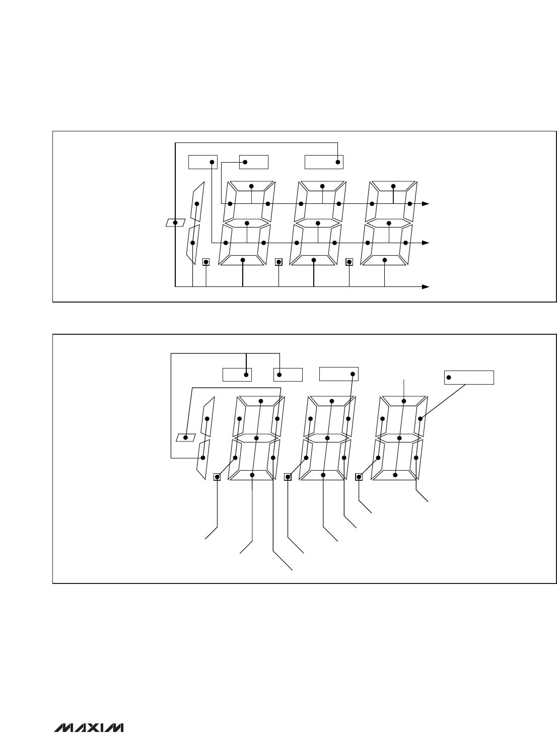
The MAX1492/MAX1494 allow for full decimal-point con-
trol and feature leading zero suppression. Use the
DP_EN, DPSET1, and DPSET2 bits in the control register
to set the value of the decimal point. Tables 2 and 3 show
the truth tables of the DP_EN, DPSET1, and DPSET2. The
truth tables determine decimal-point usage.
The MAX1492/MAX1494 overrange and underrange
display is shown in Table 4.
Reference
The MAX1492/MAX1494 reference sets the full-scale
range of the ADC transfer function. With a nominal
2.048V reference, the ADC full-scale range is ±2V with
the RANGE bit equal to 0. With the RANGE bit set to 1,
the full-scale range is ±200mV. A decreased reference
voltage decreases full-scale range (see the
Transfer
Functions
section).
The MAX1492/MAX1494 accept either an external ref-
erence or an internal reference. The INTREF bit selects
the reference mode (see the
Control Register
(Read/Write)
section).
For internal-reference operation, set INTREF to 1, con-
nect REF- to GND and bypass REF+ to GND with a
4.7µF capacitor. The internal reference provides a nom-
inal 2.048V source between REF+ and GND. The inter-
nal-reference temperature coefficient is typically
40ppm/°C.
The default power-on state sets the MAX1492/
MAX1494 to use the external reference with INTREF
cleared to 0. The external reference inputs, REF+ and
REF-, are fully differential. For a valid external-reference
input, V
REF+
must be greater than V
REF-
. Bypass REF+
and REF- with a 0.1µF or greater capacitor to GND in
external-reference mode.
3.5- and 4.5-Digit, Single-Chip ADCs
with LCD Drivers
14 ______________________________________________________________________________________