Data Sheet AD7152/AD7153
Rev. A | Page 11 of 24
SERIAL INTERFACE
The AD7152/AD7153 support an I
2
C-compatible, 2-wire serial
interface. The two wires on the I
2
C bus are called SCL (clock)
and SDA (data). These two wires carry all addressing, control,
and data information one bit at a time over the bus to all connected
peripheral devices. The SDA wire carries the data, while the
SCL wire synchronizes the sender and receiver during the
data transfer. I
2
C devices are classified as either master or slave
devices. A device that initiates a data transfer message is called a
master; a device that responds to this message is called a slave.
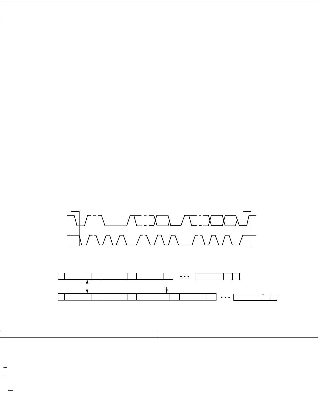
To control the AD7152/AD7153 via the bus, the following
protocol must be followed. The master initiates a data transfer
by establishing a start condition, defined by a high-to-low
transition on SDA while SCL remains high. This indicates that
the start byte follows. This 8-bit start byte is made up of a 7-bit
address plus an R/W bit indicator.
All peripherals connected to the bus respond to the start
condition and shift in the next 8 bits (7-bit address and an
R/W bit). The bits arrive MSB first. The peripheral that
recognizes the transmitted address responds by pulling the
data line low during the ninth clock pulse. This is known as the
acknowledge bit. All other devices withdraw from the bus at
this point and maintain an idle condition. An exception to this
is the general call address, which is described in the General
Call section. The idle condition is where the device monitors
the SDA and SCL lines waiting for the start condition and the
correct address byte. The R/W bit determines the direction of
the data transfer. A Logic 0 LSB in the start byte means that the
master writes information to the addressed peripheral. In this
case, the device becomes a slave receiver. A Logic 1 LSB in the
start byte means that the master reads information from the
addressed peripheral. In this case, the device becomes a slave
transmitter. In all instances, the AD7152/AD7153 act as a
standard slave device on the I
2
C bus.
The start byte address is Address 0x90 for a write and
Address 0x91 for a read.
WRITE OPERATION
When a write is selected, the byte following the start byte is
always the register address pointer (subaddress) byte, which
points to one of the internal registers on the AD7152/AD7153.
The address pointer byte is automatically loaded into the
address pointer register and acknowledged by the AD7152/
AD7153. After the address pointer byte acknowledge, a stop
condition, a repeated start condition, or another data byte can
follow from the master.
A stop condition is defined by a low-to-high transition on SDA
while SCL remains high. If a stop condition is ever encountered
by the AD7152/AD7153, it returns to its idle condition and the
address pointer is reset to Address 0x00.
If a data byte is transmitted after the register address pointer
byte, the AD7152/AD7153 load this byte into the register that
is currently addressed by the address pointer register. The devices
send an acknowledge and the address pointer autoincrementer
automatically increments the address pointer register to the
next internal register address. Thus, subsequent transmitted
data bytes are loaded into sequentially incremented addresses.
If a repeated start condition is encountered after the address
pointer byte, all peripherals connected to the bus respond
exactly as previously outlined for a start condition, that is, a
repeated start condition is treated the same as a start condition.
When a master device issues a stop condition, it relinquishes
control of the bus, allowing another master device to take
control. Hence, a master wanting to retain control of the bus
issues successive start conditions known as repeated start
conditions.
READ OPERATION
When a read is selected in the start byte, the register that is
currently addressed by the address pointer is transmitted onto
the SDA line by the AD7152/AD7153. The regulator is then
clocked out by the master device, and the AD7152/AD7153
await an acknowledge from the master.
If an acknowledge is received from the master, the address
autoincrementer automatically increments the address pointer
register and outputs the next addressed register content onto
the SDA line for transmission to the master. If no acknowledge
is received, the AD7152/AD7153 return to the idle state and the
address pointer is not incremented.
The autoincrementer of the address pointers allows block data
to be written or read from the starting address and subsequent
incremental addresses.
In continuous conversion mode, the autoincrementer of the
address pointers should be used for reading a conversion result;
that is, the three data bytes should be read using one multibyte
read transaction rather than three separate single-byte
transactions. The single-byte data read transaction may result in
the data bytes from two different results being mixed.