Data Sheet AD7152/AD7153
Rev. A | Page 7 of 24
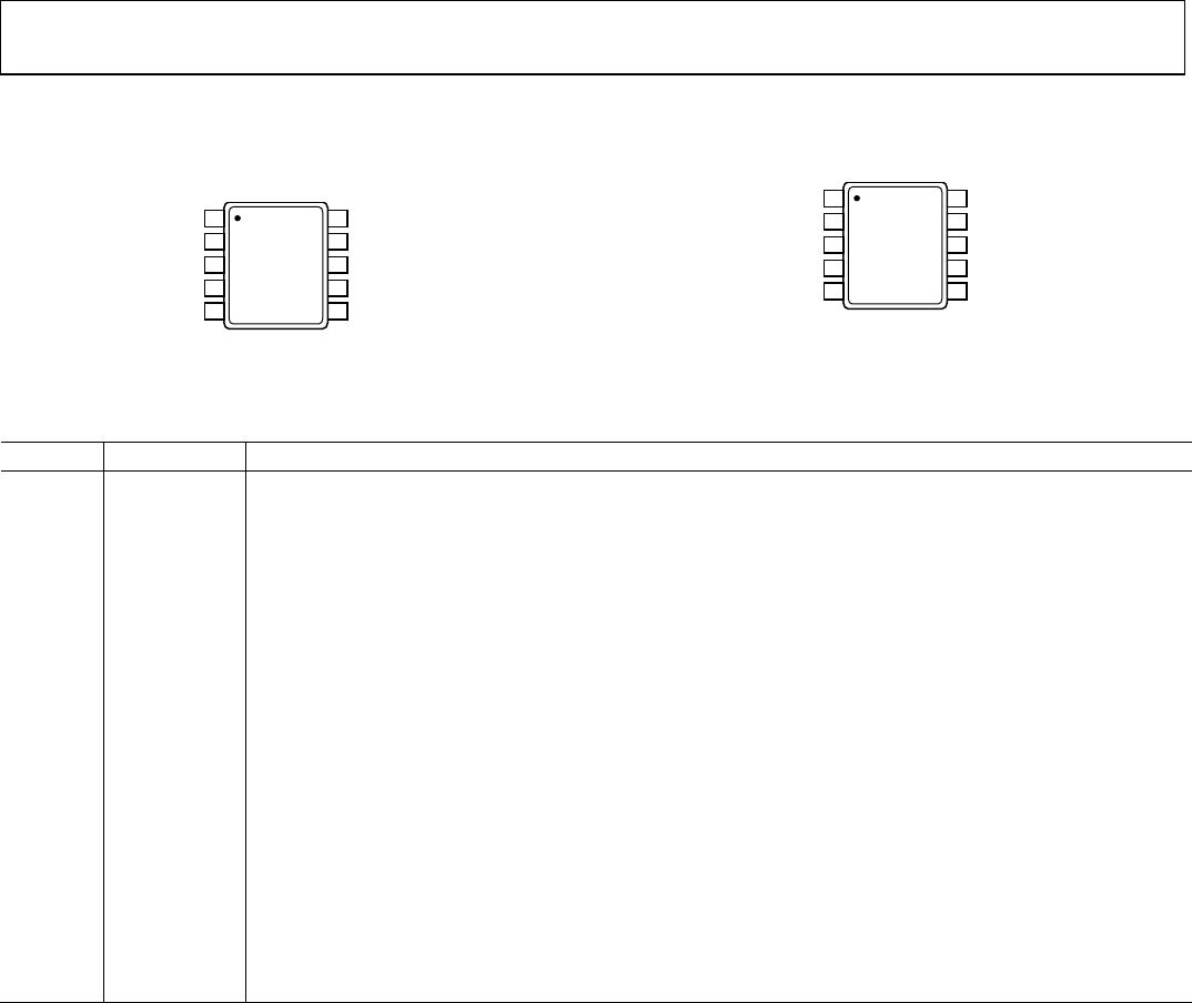
PIN CONFIGURATIONS AND FUNCTION DESCRIPTIONS
GND
1
VDD
2
CIN1(–)
3
CIN1(+)
4
EXC2
5
SDA
10
SCL
9
CIN2(–)
8
CIN2(+)
7
EXC1
6
AD7152
TOP VIEW
(Not to Scale)
07450-004
Figure 4. AD7152 Pin Configuration
NC = NO CONNECT
GND
1
VDD
2
CIN1(–)
3
CIN1(+)
4
NC
5
SDA
10
SCL
9
NC
8
NC
7
EXC1
6
AD7153
TOP VIEW
(Not to Scale)
07450-005
Figure 5. AD7153 Pin Configuration
Table 4. Pin Function Descriptions
Pin No. Mnemonic Description
1 GND Ground Pin.
2 VDD
Power Supply Voltage. This pin should be decoupled to GND, using a low impedance capacitor, for example, in
combination with a 10 μF tantalum and a 0.1 μF multilayer ceramic capacitor.
3 CIN1(–)
CDC Negative Capacitive Input of Channel 1. If not used, this pin can be left as an open circuit or connected to
GND. This pin is internally disconnected in single-ended CDC configuration.
4 CIN1(+) CDC Positive Capacitive Input of Channel 1. If not used, this pin can be left as an open circuit or connected to GND.
5 EXC2/NC
AD7152: CDC Excitation Output for Channel 2. The measured capacitance is connected between one of the EXC
pins and one of the CIN pins. If not used, these pins should be left as an open circuit.
AD7153: No Connect. This pin must be left as an open circuit.
6 EXC1
CDC Excitation Output for Channel 1. The measured capacitance is connected between one of the EXC pins and
one of the CIN pins. If not used, these pins should be left as an open circuit.
7 CIN2(+)/NC
AD7152: CDC Positive Capacitive Input of Channel 2. If not used, this pin can be left as an open circuit or
connected to GND.
AD7153: No Connect. This pin must be left as an open circuit.
8 CIN2(–)/NC
AD7152: CDC Negative Capacitive Input of Channel 2. If not used, this pin can be left as an open circuit or
connected to GND. This pin is internally disconnected in single-ended CDC configuration.
AD7153: No Connect. This pin must be left as an open circuit.
9 SCL
Serial Interface Clock Input. Connects to the master clock line. Requires a pull-up resistor if one is not already
provided in the system.
10 SDA
Serial Interface Bidirectional Data. Connects to the master data line. Requires a pull-up resistor if one is not
provided elsewhere in the system.
AD7152/AD7153 Data Sheet
Rev. A | Page 8 of 24
TYPICAL PERFORMANCE CHARACTERISTICS
0.05
0.04
0.03
0.02
0.01
0
0.01
0.02
0.03
0.04
0.05
–2 –1
0
1
2
CAPACITANCE (pF)
INL (% of FSR)
07450-106
Figure 6. Capacitance Input Integral Nonlinearity,
V
DD
= 3.3 V, See Figure 34
–0.25
–0.20
–0.15
–0.10
–0.05
0.00
0.05
0.10
0.15
0.20
50 25
0
25 50
75 100
TEMPERATURE (°C)
GAIN ERROR (%FSR)
07450-107
TC ≈ 28ppm/°C
Figure 7. Capacitance Input Gain Drift vs. Temperature,
V
DD
= 3.3 V, Range = ±2 pF
–0.4
–0.2
0
0.2
0.4
–50 –25 0 25 50 75 100
TEMPERATURE (°C)
OFFSET CAPACITANCE (fF)
07450-108
Figure 8. Capacitance Input Offset Drift vs. Temperature,
V
DD
= 3.3 V, CIN and EXC Pins Open Circuit
12
1
0
–8
–6
–4
–2
0
2
0
5
0
10
0
15
0
200 250 300 350
CAP LOA
D T
O
G
ND
(
p
F
)
GAIN ERROR (%FSR)
3
p
F
9
p
F
07450-109
Figure 9. Capacitance Input Error vs. Capacitance Between CIN and GND;
Single-Ended Mode, CIN(+) to EXC = 3 pF and 9 pF, V
DD
= 3.3 V
–12
–10
–8
–6
–4
–2
0
2
0 50 100
150 200 250 300 350
CAP LOAD TO GND (pF)
GAIN ERROR (%FSR)
2pF
07450-110
8pF
Figure 10. Capacitance Input Error vs. Capacitance Between CIN and GND,
Differential Mode, CIN(+) to EXC = 2 pF and 8 pF,
CIN(−) to EXC = 0 pF and 6 pF, V
DD
= 3.3 V
–0.3
–0.2
–0.1
0
0.1
0.2
0.3
0 50 100 150 200 250 300 350
CAP LOAD TO GND (pF)
GAIN ERROR (%FSR)
07450-111
Figure 11. Capacitance Input Error vs. Capacitance Between EXC and GND,
Single-Ended Mode, CIN(+) to EXC = 9 pF, V
DD
= 3.3 V
Data Sheet AD7152/AD7153
Rev. A | Page 9 of 24
–0.3
–0.2
–0.1
0
0.1
0.2
0.3
0 50
100
150 200 250 300 350
CAP LOAD TO GND (pF)
GAIN ERROR (%FSR)
07450-112
Figure 12. Capacitance Input Error vs. Capacitance Between EXC and GND,
Differential Mode, CIN(+) to EXC = 8 pF,
CIN(−) to EXC = 6 pF, V
DD
= 3.3 V
–10
–8
–6
–4
–2
0
2
1 10 100 1000
RESISTANCE CIN TO GROUND (MΩ)
GAIN ERROR (%FSR)
07450-113
Figure 13. Capacitance Input Error vs. Parasitic Resistance CIN to GND,
Single-Ended Mode, CIN(+) to EXC = 9 pF, VDD = 3.3 V
–0.6
–0.4
–0.2
0
0.2
0.4
0.6
1 10 100 1000
RESISTANCE EXC TO GROUND (MΩ)
GAIN ERROR (%FSR)
07450-114
Figure 14. Capacitance Input Error vs. Parasitic Resistance EXC to GND,
Single-Ended Mode, CIN(+) to EXC = 9 pF, VDD = 3.3 V
–50
–40
–30
–20
–10
0
10
1 10
100 1000
PARALLEL RESISTANCE (MΩ)
GAIN ERROR (%FSR)
07450-115
Figure 15. Capacitance Input Error vs. Parasitic Parallel Resistance
Single-Ended Mode, CIN(+) to EXC = 9 pF, VDD = 3.3 V
–30
–25
–20
–15
–10
–5
0
0
20 40
60 80 100
SERIAL RESISTANCE (kΩ)
GAIN ERROR (%FSR)
3pF
9pF
07450-116
Figure 16. Capacitance Input Error vs. Serial Resistance,
Single-Ended Mode, CIN(+) to EXC = 3 pF and 9 pF, VDD = 3.3 V
–1.0
–0.8
–0.6
–0.4
–0.2
0.0
0.2
2.6 2.8 3.0 3.2 3.4 3.6 3.8
VDD (V)
GAIN ERROR (fF)
07450-117
Figure 17. Capacitance Input Power Supply Rejection (PSR),
Differential Mode; CIN(+) to EXC = 1.9 pF

AD7153BRMZ-REEL

Mfr. #:
Manufacturer:
Analog Devices Inc.
Description:
Data Acquisition ADCs/DACs - Specialized 1-CH 12-bit CDC IC
Lifecycle:
New from this manufacturer.
Delivery:
DHL FedEx Ups TNT EMS
Payment:
T/T Paypal Visa MoneyGram Western Union

Products related to this Datasheet