Data Sheet AD7152/AD7153
Rev. A | Page 19 of 24
CAPDAC
The CDC full-scale input range of the AD7152/AD7153 can
be set to ±0.25 pF, ±0.5 pF, ± 1 pF, and ±2 pF in differential
mode or 0.5 pF, 1 pF, 2 pF, and 4 pF in single-ended mode.
For simplicity, the following text and figures use the maximum
full scale of ±2 pF and +4 pF.
The devices can accept a higher capacitance on the input and
the common-mode or offset capacitance (unchanging component)
can be balanced by programmable on-chip CAPDACs.
DATA
CDC
EXC
CIN(+)
CIN(–)
C
X
CAPDAC(+)
CAPDAC(–)
C
Y
07450-010
Figure 28. Using a CAPDAC
The CAPDAC can be understood as a negative capacitance
connected internally to the CIN pin. There are two independent
CAPDACs, one connected to the CIN(+) and the second
connected to the CIN(–).
In differential mode, the relationship between the capacitance
input and output data can be expressed as
DATA ≈ (C
X
CAPDAC(+)) − (C
Y
CAPDAC(−))
In single-ended mode, the relationship between the capacitance
input and output data can be expressed as
DATAC
X
−(CAPDAC(+) + CAPDAC(−))
The CAPDACs have a 5-bit resolution each, monotonic transfer
function, are well matched to each other, and have a defined
temperature coefficient. The CAPDAC full range (absolute
value) is not factory calibrated and can vary up to ±20% with
the manufacturing process (see the Specifications section,
Figure 18, and Figure 19).
The CAPDACs are shared by the two capacitive channels on the
AD7152. If the CAPDACs need to be set individually, the host
controller software should reload the CAPDAC values to the
AD7152 before executing a conversion on a different channel.
SINGLE-ENDED CAPACITIVE INPUT
When configured for a single-ended mode (the CAPDIFF bit in
the Channel 1 Setup or Channel 2 Setup registers is set to 0), the
AD7152/AD7153 CIN(−) pin is disconnected internally. The
CDC (without using the CAPDACs) can measure positive input
capacitance in the range of 0 pF to 4 pF (see Figure 29).
0x0000 ... 0xFFF0
DATA
CAPDIFF = 0
0pF TO 4pF
CDC
EXC
CIN(+)
CIN(–)
C
X
0pF TO 4pF
CAPDAC(+)
OFF
CAPDAC(–)
OFF
07450-024
Figure 29. CDC Single-Ended Input Mode
The CAPDAC can be used for programmable shifting of the
input range.
Figure 30 shows how to shift the input range up to 9 pF absolute
value of capacitance connected to the CIN(+) using
the CAPDAC(+) only.
0x0000 ... 0xFFF0
DATA
CAPDIFF = 0
0pF TO 4pF
CDC
EXC
CIN(+)
CIN(–)
C
X
5pF TO 9pF
CAPDAC(+)
5pF
CAPDAC(–)
OFF
07450-124
Figure 30. Using CAPDAC in Single-Ended Mode
Figure 31 shows how to shift the input range up to 14 pF
absolute value of capacitance connected to the CIN(+) using
both CAPDAC(+) and CAPDAC(−).
0x0000 ... 0xFFF0
DATA
CAPDIFF = 0
0pF TO 4pF
CDC
EXC
CIN(+)
CIN(–)
C
X
10pF TO 14pF
CAPDAC(+)
5pF
CAPDAC(–)
5pF
07450-224
Figure 31. Using CAPDAC in Single-Ended Mode
AD7152/AD7153 Data Sheet
Rev. A | Page 20 of 24
DIFFERENTIAL CAPACITIVE INPUT
When configured for differential mode (the CAPDIFF bit in the
Channel 1 Setup or Channel 2 Setup registers is set to 1), the
CDC measures the difference between positive and negative
capacitance input.
Each of the two input capacitances, C
X
and C
Y
, between the
EXC and CIN pins must be less than 2 pF (without using the
CAPDACs) or must be less than 9 pF and balanced by the
CAPDACs. Balancing by the CAPDACs means that both
C
X
− CAPDAC(+) and C
Y
− CAPDAC(−) are less than 2 pF.
If the unbalanced capacitance between the EXC and CIN pins
is higher than 2 pF, the CDC introduces a gain error, an offset
error, and nonlinearity error (see Figure 32, Figure 33, and
Figure 34).
0x0000 ... 0xFFF0
DATA
CAPDIFF = 1
±2pF
CDC
EXC
CIN(+)
CIN(–)
C
X
0pF TO 4pF
C
Y
0pF TO 4pF
CAPDAC(+)
OFF
CAPDAC(–)
OFF
07450-020
Figure 32. CDC Differential Input Mode
0x0000 ... 0xFFF0
DATA
CAPDIFF = 1
±2pF
CDC
EXC
CIN(+)
CIN(–)
C
X
4pF TO 6pF
(5 ± 1pF)
C
Y
4pF TO 6pF
(5 ± 1pF)
CAPDAC(+)
5pF
CAPDAC(–)
5pF
07450-021
Figure 33. Using CAPDAC in Differential Mode
0x0000 ... 0xFFF0
DATA
CAPDIFF = 1
±2pF
CDC
EXC
CIN(+)
CIN(–)
C
X
3pF TO 7pF
(5 ± 2pF)
C
Y
5pF
CAPDAC(+)
5pF
CAPDAC(–)
5pF
07450-121
Figure 34. Using CAPDAC in Differential Mode
PARASITIC CAPACITANCE TO GROUND
DATA
CDC
EXC
C
GND1
CIN
C
GND2
C
X
07450-012
Figure 35. Parasitic Capacitance to Ground
The CDC architecture used in the AD7152/AD7153 measures
C
X
connected between the EXC pin and the CIN pin. In theory,
any capacitance, C
GND
, to ground should not affect the CDC
result (see Figure 35).
The practical implementation of the circuitry in the chip
implies certain limits and the result is gradually affected by
capacitance to ground. See the allowed capacitance to GND
in the Specifications table and, Figure 9 through Figure 12.
PARASITIC RESISTANCE TO GROUND
DATA
CDC
EXC
R
GND1
CIN
R
GND2
C
X
07450-013
Figure 36. Parasitic Resistance to Ground
The CDC result can be affected by a leakage current from the
C
X
to ground; therefore, the C
X
should be isolated from the
ground. The influence of the leakage current varies with the
power supply voltage (see Figure 36).
A higher leakage current to ground results in a gain error, an
offset error, and a nonlinearity error (see Figure 13 and Figure 14).
Data Sheet AD7152/AD7153
Rev. A | Page 21 of 24
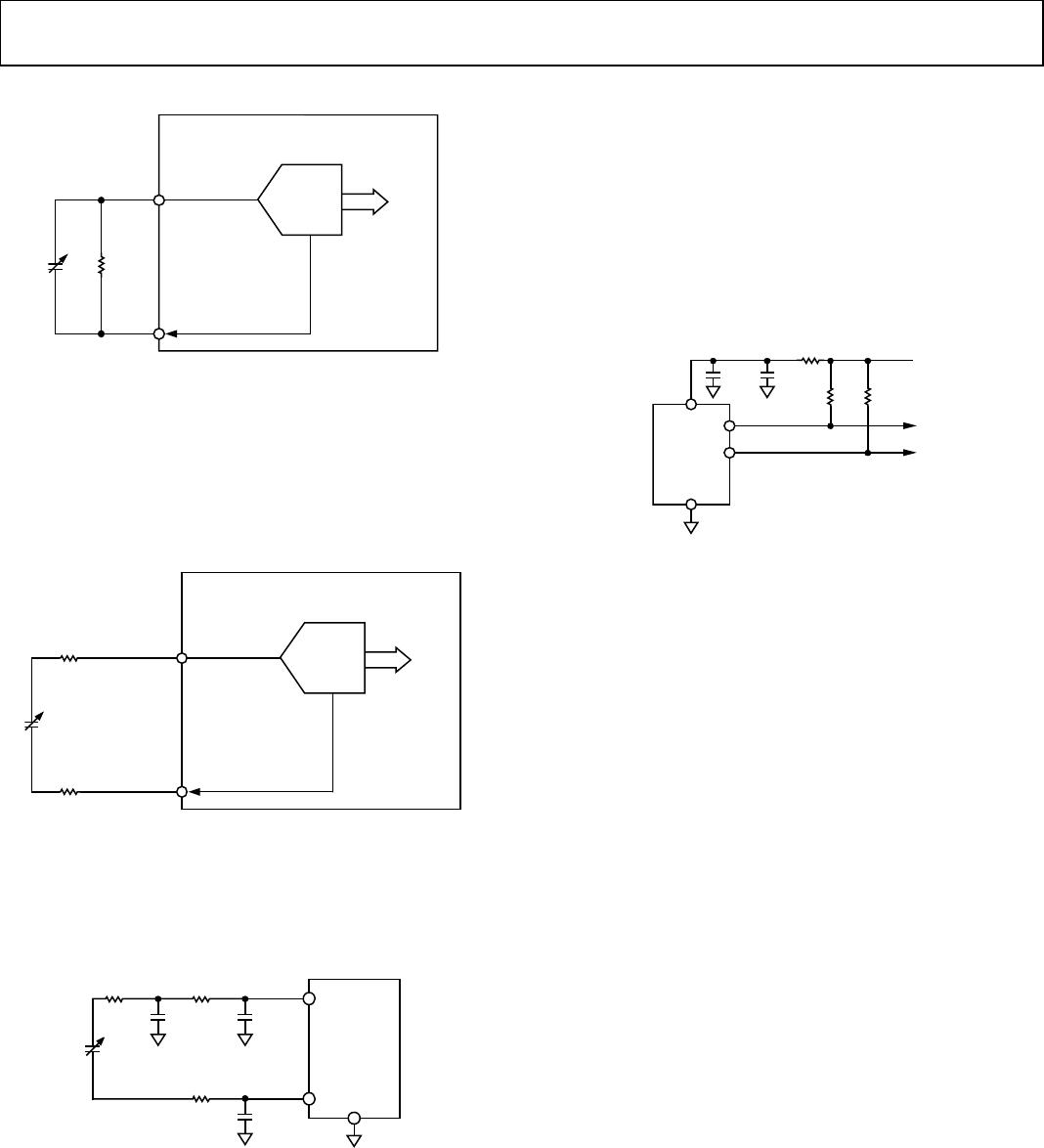
PARASITIC PARALLEL RESISTANCE
DATA
CDC
EXC
CIN
R
P
07450-022
C
X
Figure 37. Parasitic Parallel Resistance
The CDC measures the charge transfer between the EXC pin
and CIN pin. Any resistance connected in parallel to the meas-
ured capacitance C
X
(see Figure 37), such as the parasitic
resistance of the sensor, also transfers charge. Therefore, the
parallel resistor is seen as an additional capacitance in the
output data causing a capacitive input error (see Figure 15).
PARASITIC SERIAL RESISTANCE
DATA
CDC
EXC
R
S1
CIN
R
S2
C
X
07450-023
Figure 38. Parasitic Serial Resistance
The CDC result is affected by a resistance in series with the
measured capacitance. The total serial resistance, which refers
to R
S1
and R
S2
in Figure 38, should be less than 20 kΩ for the
specified performance (see Figure 16).
INPUT EMC PROTECTION
CDC
GND
07450-039
CIN
EXC
C2
C3
C
X
R3
R2R1
C1
Figure 39. AD7152/AD7153 EMC Protection
Some applications may require an additional input filter for
improving electromagnetic compatibility (EMC). Any input
filter must be carefully designed, considering the balance between
the system capacitance performance and system electromagnetic
immunity.
Figure 39 shows one of the possible input circuit configurations
significantly improving the system immunity against high fre-
quency noise and slightly affecting the AD7152 performance in
terms of additional gain and offset error.
POWER SUPPLY DECOUPLING AND FILTERING
CDC
GND
SDA
SCL
0.1µF 10µF
1k
V
DD
1k 1k
0
7450-058
Figure 40. AD7152/AD7153 V
DD
Decoupling and Filtering
The AD7152 has good dc and low frequency power supply
rejection but may be sensitive to higher frequency ripple and
noise, specifically around the excitation frequency and its
harmonics. Figure 40 shows a possible circuit configuration
for improving the system immunity against ripple and noise
coupled to the AD7152 via the power supply.
Because the serial interface is connected to the other circuits in
the system, it is better to connect the pull-up resistors on the
other side of the V
DD
filter than to connect to the AD7152.
CAPACITIVE GAIN CALIBRATION
The gain of the AD7152/AD7153 is factory calibrated for the full
scale of 4 pF in the production for each device individually. The
factory gain coefficient is stored in a one-time programmable
(OTP) memory and is copied to the capacitive gain registers at
power-up or after reset.
The gain can be changed by executing a capacitance gain
calibration mode, for which an external full-scale capacitance
needs to be connected to the capacitance input, or by writing a
user value to the capacitive gain register. This change is tempo-
rary and the factory gain coefficient can be reloaded after
power-up or reset. The device is tested and specified only for
use with the default factory calibration coefficient.
CAPACITIVE SYSTEM OFFSET CALIBRATION
The capacitive offset is dominated by the parasitic offset in the
application, such as the initial capacitance of the sensor, any
parasitic capacitance of tracks on the board, and the capacitance
of any other connections between the sensor and the CDC.
Therefore, the AD7152/AD7153 are not factory calibrated for
capacitive offset. The user should calibrate the system capacitance
offset in the application.

AD7153BRMZ-REEL

Mfr. #:
Manufacturer:
Analog Devices Inc.
Description:
Data Acquisition ADCs/DACs - Specialized 1-CH 12-bit CDC IC
Lifecycle:
New from this manufacturer.
Delivery:
DHL FedEx Ups TNT EMS
Payment:
T/T Paypal Visa MoneyGram Western Union

Products related to this Datasheet