Data Sheet AD7152/AD7153
Rev. A | Page 15 of 24
DATA REGISTERS
Address 0x01, Address 0x02 for Channel 1,
Address 0x03, Address 0x04 (AD7152 Only) for Channel 2,
16 Bits, Read-Only, Default Value 0x0000
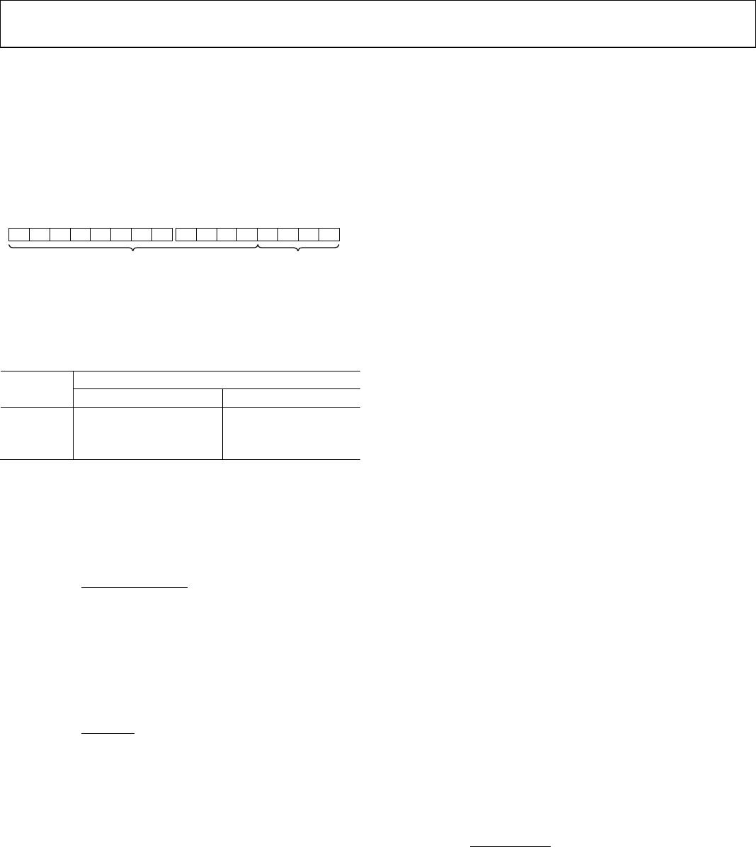
Data from the last complete capacitance-to-digital conversion
reflects the capacitance on the input. Only the 12 MSBs of the
data registers are used for the CDC result. The 4 LSBs are
always 0, as shown in Figure 24.
BIT 7
BIT 6 BIT 5
BIT 4 BIT 3 BIT 2
12-BIT CDC RESULT
BIT 1 BIT 0
BIT 7
BIT 6
BIT 5
BIT 4
BIT 3
BIT 2
DATA HIGHMSB DATA LOW LSB
BIT 1
BIT 0
0
07450-044
Figure 24. CDC Data Register
The AD7152/AD7153 are factory gain calibrated and map the
CDC full-scale raw data range of 0x3000 to 0xCFF0 to a CDC
full-scale data register range of 0x0000 to 0xFFF0 (see Table 9).
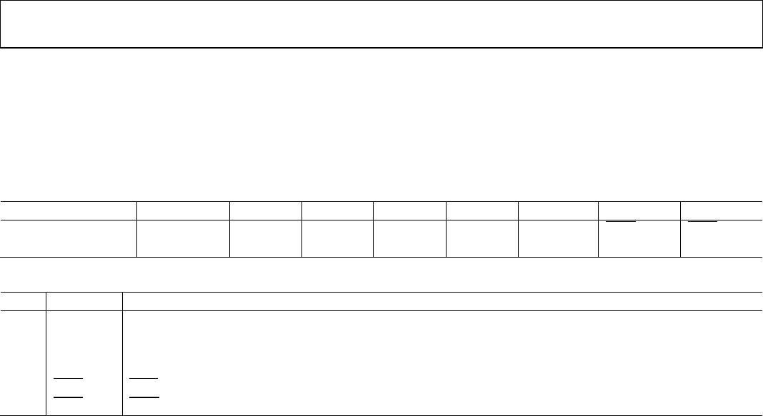
Table 9. AD7152/AD7153 Capacitance-to-Data Mapping
Data Reg
Input Capacitance (4 pF range)
Differential Mode Single-Ended Mode
Negative full scale (–2 pF)
0x8000 Zero scale (0 pF) Midscale (2 pF)
0xFFF0 Positive full scale (+2 pF) Full scale (4 pF)
The data register output in differential mode is internally
calculated using the following equation:
Data Reg = (Code – (Offset Reg – 0x8000)) × Gain + 0x8000 (1)
The input capacitance can be calculated from the output data
using the following equation:
RangeInput
xRegData
C ×
−
=
0xFFF0
80000
(pF)
(2)
The data register output in single-ended mode is internally
calculated using the following equation:
Data Reg = (Code − (Offset Reg − 0x3000)) × Gain (3)
The input capacitance can be calculated from the output data
using the following equation:
RangeInput
RegData
C ×=
0
xFFF0
(pF)
(4)
where Input Range = 4 pF, 2 pF, 1 pF, or 0.5 pF.
A data register is updated after a finished conversion on the
capacitive channel, with one exception: when the serial interface
read operation from the data register is in progress, the data
register is not updated and the new capacitance conversion
result is lost.
The stop condition on the serial interface is considered to be the
end of the read operation.
Therefore, to prevent incorrect data reading through the
serial interface, the two bytes of a data register should be
read sequentially using the register address pointer auto-
increment feature of the serial interface.
OFFSET CALIBRATION REGISTERS
Address 0x05, Address 0x06 for Channel 1,
Address 0x07, Address 0x08 for Channel 2 (AD7152 Only)
16 Bits Read/Write, Default Value 0x8000
The offset calibration registers hold the zero-scale calibration
coefficients.
The zero-scale calibration coefficient digitally maps the zero
capacitance on the CDC input to the zero-scale data code.
The coefficient can be used for compensation of the AD7152/
AD7153 internal offset as well as the system level offset within
specified offset calibration limits.
Users can set the coefficient by executing the offset calibration
after connecting the zero-scale capacitance to the system input.
Alternatively, the coefficient value can be written to the offset
calibration register(s) by the host software, for example, values
stored in a host nonvolatile memory.
Note that there is a difference between code mapping in differ-
ential and single-ended input mode. In differential mode, the
nominal zero-scale calibration coefficient value is a power-on
default, 0x8000. In single–ended mode, the nominal zero-scale
calibration coefficient value is 0x3000.
The difference means that before using the single-ended mode
(or any time when changing between modes afterwards), the
user should either perform offset calibration with capacitance
close to 0 pF connected to the input or write the offset calibra-
tion register(s) value(s) close to 0x8000 for differential mode or
value close to 0x3000 for single-ended mode.
On the AD7152, the two capacitive channels have individual
offset registers and each channel can be calibrated individually.
GAIN CALIBRATION REGISTERS
Address 0x09, Address 0x0A for Channel 1
Address 0x0C, Address 0x0D for Channel 2 (AD7152 Only)
16 Bits Read/Write, Default Value 0xXXXX
The capacitive gain calibration registers hold the capacitive
channel full-scale factory calibration coefficient. The gain
calibration factor can be calculated using the following
equation:
16
16
2
2 RegGain
Gain
+
=
(5)
On the AD7152, the two capacitive channels each have a gain
register, which allows the device to gain calibrate each channel
individually.