AD7152/AD7153 Data Sheet
Rev. A | Page 4 of 24
Parameter Min Typ Max Unit
1
Test Conditions/Comments
POWER REQUIREMENTS
V
DD
-to-GND Voltage 2.7 3.6 V V
DD
= 3.3 V, nominal
Current, I
DD
9
100 120 µA
Current Power-Down Mode, I
DD
9
1 5 µA Temperature ≤ 25°C
3
10
µA
Temperature = 85°C
1
Capacitance units: 1 pF = 10
12
F; 1 fF = 10
−15
F; 1 aF = 10
−18
F.
2
Specification is not production tested but is supported by characterization data at initial product release.
3
Except Channel 2 in differential mode. To achieve the specified performance in differential mode, the I
2
C interface must be idle during the capacitance conversion to
prevent signal coupling from the SCL pin to the adjacent CIN2() pin.
4
Factory calibrated. The absolute error includes factory gain calibration error and integral nonlinearity error all at 2C. At different temperatures, compensation for
gain drift over temperature is required.
5
Specification is not production tested but guaranteed by design.
6
A system offset calibration is effectively a conversion; therefore, the offset error is of the order of the conversion noise. This applies after calibration at the temperature,
capacitive input range, and applied V
DD
of interest. The capacitive input offset can be reduced using a system offset calibration. Large offsets should be removed using
CAPDACs.
7
The gain error is factory calibrated at 25°C. At different temperatures, compensation for gain drift over temperature is required.
8
The CAPDAC resolution is five bits in the actual CAPDAC full range. Using the on-chip offset calibration or adjusting the capacitive offset calibration register can
further reduce the CIN offset or the unchanging CIN component.
9
Digital inputs equal to V
DD
or GND.
Data Sheet AD7152/AD7153
Rev. A | Page 5 of 24
TIMING SPECIFICATIONS
V
DD
= 2.7 V to 3.6 V; GND = 0 V; Input Logic 0 = 0 V; Input Logic 1 = V
DD
; −40°C to +85°C, unless otherwise noted.
Table 2.
Parameter Min Typ Max Unit Test Conditions/Comments
SERIAL INTERFACE
1, 2
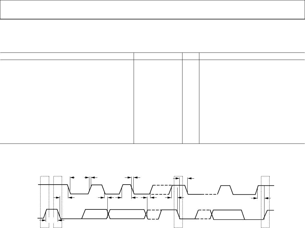
See Figure 3.
SCL Frequency 0 400 kHz
SCL High Pulse Width, t
HIGH
0.6 µs
SCL Low Pulse Width, t
LOW
1.3 µs
SCL, SDA Rise Time, t
R
0.3 µs
SCL, SDA Fall Time, t
F
0.3
µs
Hold Time (Start Condition), t
HD;STA
0.6 µs After this period, the first clock is generated.
Set-Up Time (Start Condition), t
SU;STA
0.6 µs Relevant for repeated start condition.
Data Set-Up Time, t
SU;DAT
0.1 µs
Setup Time (Stop Condition), t
SU;STO
0.6 µs
Data Hold Time, t
HD;DAT
(Master) 0.01 µs
Bus-Free Time (Between Stop and Start Conditions, t
BUF
)
µs
1
Sample tested during initial release to ensure compliance.
2
All input signals are specified with input rise/fall times = 3 ns, measured between the 10% and 90% points. Timing reference points at 50% for inputs and outputs;
output load = 10 pF.
P
S
t
LOW
t
R
t
F
t
HD;STA
t
HD;D
AT
t
SU;DA
T
t
SU;S
TA
t
HD;STA
t
SU;STO
t
HIGH
SCL
P
S
SDA
t
BUF
07450-003
Figure 3. Serial Interface Timing Diagram
AD7152/AD7153 Data Sheet
Rev. A | Page 6 of 24
ABSOLUTE MAXIMUM RATINGS
T
A
= 25°C, unless otherwise noted.
Table 3.
Parameter Rating
Positive Supply Voltage, V
DD
to GND 0.3 V to +3.9 V
Voltage on Any Input or Output Pin to GND
0.3 V to V
DD
+ 0.3 V
ESD Rating (ESD Association Human
Body Model, S5.1)
4 kV
ESD Rating (Field-Induced Charged
Device Model)
750 V
Operating Temperature Range −40°C to +85°C
Storage Temperature Range −65°C to +150°C
Junction Temperature 150°C
MSOP
θ
JA
Thermal Impedance-to-Air 206°C/W
θ
JC
Thermal Impedance-to-Case 44°C/W
Reflow Soldering (Pb-Free)
Peak Temperature 260 (+0/−5)°C
Time at Peak Temperature 10 sec to 40 sec
Stresses at or above those listed under Absolute Maximum
Ratings may cause permanent damage to the product. This is a
stress rating only; functional operation of the product at these
or any other conditions above those indicated in the operational
section of this specification is not implied. Operation beyond
the maximum operating conditions for extended periods may
affect product reliability.
ESD CAUTION

AD7153BRMZ-REEL

Mfr. #:
Manufacturer:
Analog Devices Inc.
Description:
Data Acquisition ADCs/DACs - Specialized 1-CH 12-bit CDC IC
Lifecycle:
New from this manufacturer.
Delivery:
DHL FedEx Ups TNT EMS
Payment:
T/T Paypal Visa MoneyGram Western Union

Products related to this Datasheet