1©2017 Integrated Device Technology, Inc. October 24, 2017
Description
The 5L2503 MicroClock programmable clock generator is
intended for low-power, consumer, wearable and smart devices.
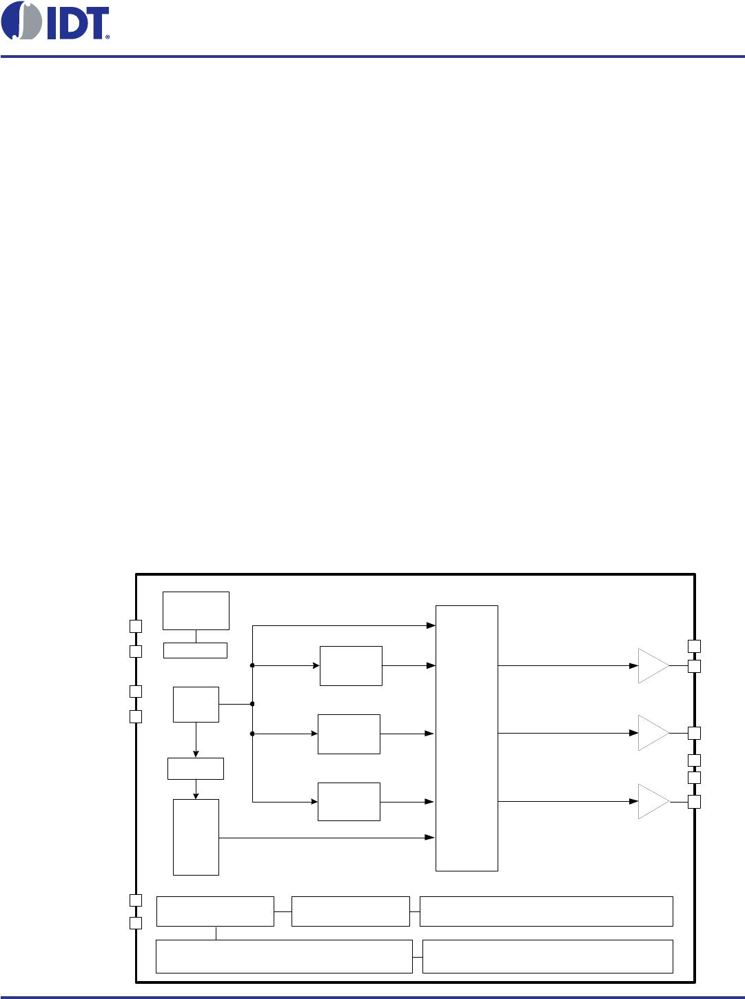
The 5L2503 device is a 3 PLL architecture design. Each PLL is
individually programmable, allowing up to 3 unique frequency
outputs. The 5L2503 has built-in unique features such as
Proactive Power Saving (PPS) to deliver better system level
power management.
An internal OTP memory allows the user to store the configuration
in the device without programming after power-up, and then can
be reprogrammed again through the I
2
C interface.
The device has programmable VCO and PLL source selection
allowing the user to do power-performance optimization based on
the application requirements. A low-power 32.768kHz clock is
supported with only less than 2μA current consumption for system
RTC reference clock needs.
Typical Applications
SmartDevice
Handheld
Wearable applications
Consumer application crystal replacements
Features
Configurable OE1 pin function as OE, PPS or DFC control
function
Proactive Power Saving (PPS) features save power during the
end device power down mode
Dynamic Frequency Control (DFC) feature allows programming
up to 4 difference frequencies switch dynamically
Spread spectrum clock support to lower system EMI
I
2
C Interface
Output Features
3 LVCMOS outputs: 1MHz–125MHz
Low Power 32.768kHz clock supported
Wireless clock crystal integration and fan out directly
Key Specifications
2μA operation for RTC clock 32.768kHz output
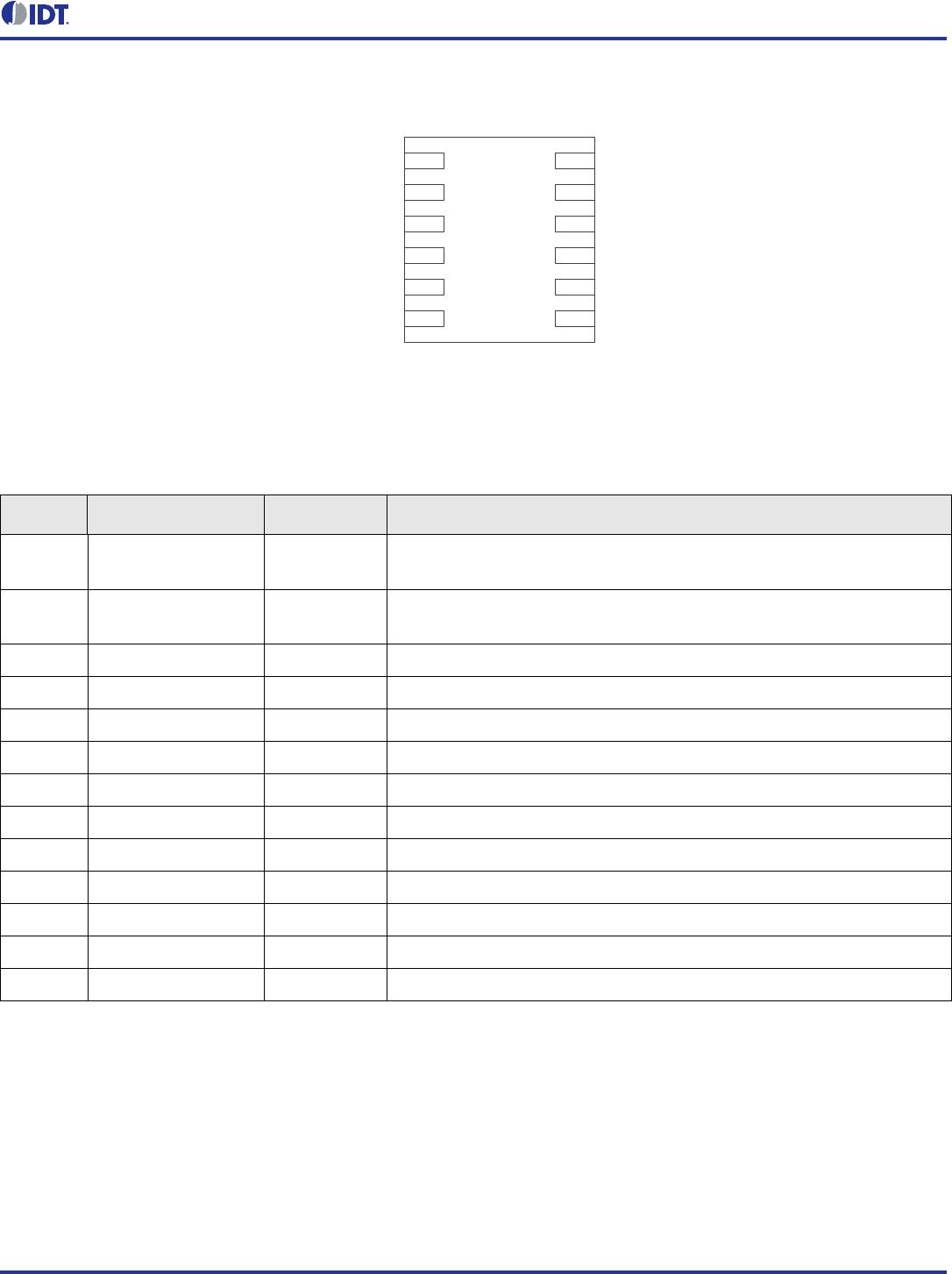
2.5 × 2.5 mm 12-DFN small form factor package
Block Diagram
Overshoot Reduction
(ORT)
OSC
PLL2
OUT3
OUT2
OUT1
PLL3
OE1
SDA_DFC0/OE2
SEL_DFC/ SCL_DFC1/OE3
OTP memory (1 configuration ) Proactive Power Saving Logic (PPS)
I
2
C Engine Dynamic Frequency Control Logic (DFC)
POR
Power
Monitor
VDD1_8
32.768K
DCO
Calibration
VSS
VDDO
PLL1
VSS
Mux
&
Divider
XOUT
CLKIN / XIN
5L2503
Datasheet
MicroClock Programmable Clock
Generator
2©2017 Integrated Device Technology, Inc. October 24, 2017
5L2503 Datasheet
Pin Assignments
Figure 1. Pin Assignments for 2.5 × 2.5 mm 12-DFN – Top View
Pin Descriptions
Table 1. Pin Descriptions
Number Name Type Description
1 SDA_DFC0/OE2 I/O
I
2
C data pin; can be DFC0 function by OTP programming or selected by
SEL_DFC at power-on default. Output enable pin for OUT2.
2
SEL_DFC/SCL_DFC1/
OE3
Input
I
2
C clock pin; can be DFC1 function by OTP programming selected by
SEL_DFC at power-on default. Output enable pin for OUT3.
3V
SS
Power Ground pin.
4 XOUT I/O Crystal oscillator interface output.
5
XIN Input Crystal oscillator interface input or clock input pin (CLKIN).
6 V
DD1_8
Power 1.8V power rail.
7 OUT1 Output 1.8V LVCMOS clock output.
8
OE1 Input Output enable control 1.
9 OUT2 Output 1.8V LVCMOS clock output.
10 V
DDO
Power 1.8V output clock power supply pin; supports OUT2/3.
11
OUT3 Output 1.8V LVCMOS clock output.
12
V
SS
Power Ground pin.
EPAD Power Connect to ground pad.
SDA_DFC0/OE2
SEL_DFC/SCL_DFC1/OE3
VSS
XOUT
XIN
VDD1_8 OUT1
OE1
OUT2
VDDO
OUT3
VSS1
2
3
4
5
67
8
9
10
11
12
2.5 × 2.5 mm 12-DFN
3©2017 Integrated Device Technology, Inc. October 24, 2017
5L2503 Datasheet
Power Group
Output Source Selection Register Settings
Table 4. OUT2 Source
Table 5. OUT1 Source
Table 6. DIV1 Source
Table 2. Power Group
Power Supply SE DIV MUX PLL DCO XTAL
V
DDO
OUT2/OUT3 V
V
DD1_8
OUT1 V V V V
Table 3. OUT3 Source
OUT3 Source B35b7 B35b6
Divider 3 (DIV3) 0 0
Divider 5 (DIV5) 0 1
Divider 1 (DIV1) 1 0
32.768kHz DCO 1 1
OUT2 Source B35b5 B35b4
Divider 3 (DIV3) 0 0
Divider 5 (DIV5) 0 1
Divider 1 (DIV1) 1 0
32.768kHz DCO 1 1
OUT1 source B35b3 B35b2
Divider 3 (DIV3) 0 0
Divider 5 (DIV5) 0 1
Divider 1 (DIV1) 1 0
32.768kHz DCO 1 1
DIV1 source B35b1 B35b0
PLL1 0 0
DIV4 seed 1 X

5L2503-000NVGI

Mfr. #:
Manufacturer:
IDT
Description:
Clock Generators & Support Products Microclock Programmable Clock Generator
Lifecycle:
New from this manufacturer.
Delivery:
DHL FedEx Ups TNT EMS
Payment:
T/T Paypal Visa MoneyGram Western Union

Products related to this Datasheet