6©2017 Integrated Device Technology, Inc. October 24, 2017
5L2503 Datasheet
Input Pin Function
The input pins in 5L2503 have multiple functions. The OE1 pin can be configured as output enable control (OE) or chip power-down
control (PD#) or Proactive Power Saving function (PPS). Furthermore, the OE1 pin can be configured as a single or two-pin Dynamic
Frequency Control (DFC).
SCL/SDA are also multiple function pins. The two pins can be configured as output enable control (OE), or I
2
C interface or Dynamic
Frequency Control (DFC) functions by programming and hardware pin latch.
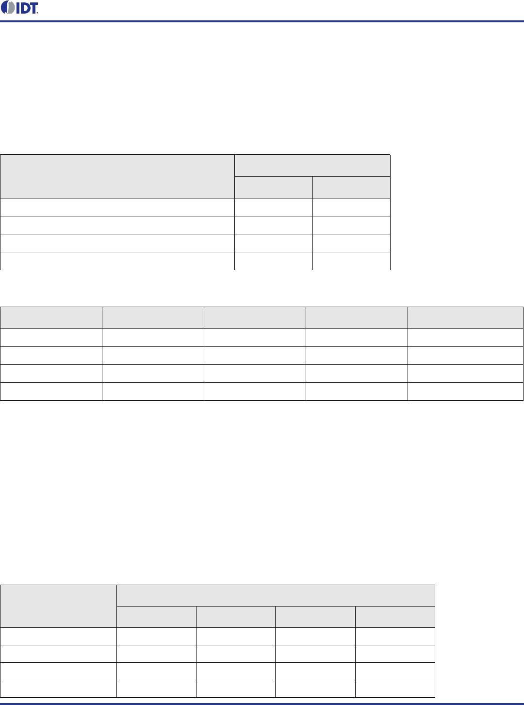
Table 8. OE1 Pin Function
Table 9. SDA/SCL Function
Spread Spectrum
The 5L2503 supports spread spectrum clocks from PLL1. PLL1 has built-in analog spread spectrum; PLL2 and PLL3 use seed clock from
PLL1.
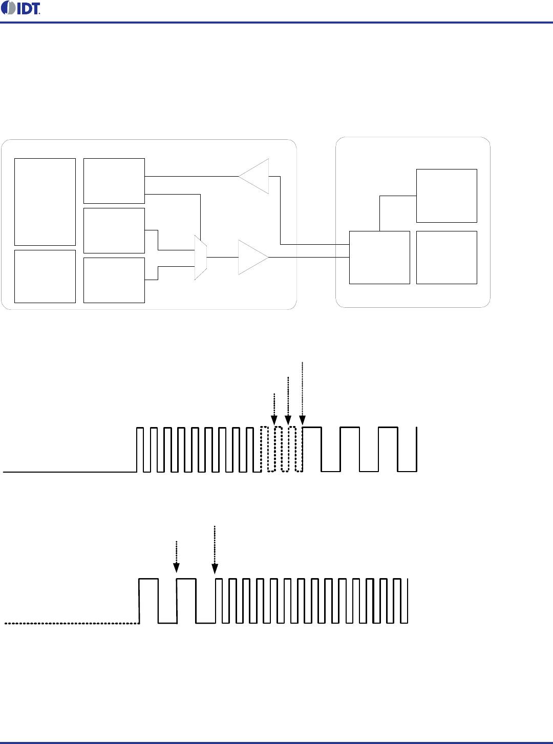
ORT – VCO Overshoot Reduction Technology
The 5L2503 supports innovate the VCO overshoot reduction technology to prevent the output clock frequency spike when the device is
change frequency on the fly or doing DFC (Dynamic Frequency Control) function. The VCO frequency change are under control instead
of freerun to targeted frequency.
PLL Features and Descriptions
Table 10. Output Divider 1
Function
Byte30
bit6 bit5
OUT1 output enable/disable 0 0
Global Power Down (PD#) 0 1
OUT1 Proactive Power Saving Input (OUT1 PPS) 1 0
DFC0 1 1
SEL_DFC (latched) Enable OE2/3 B36<2> DFC_EN B32<4> OE1 Funsel B30<6:5> Function of SCL/SDA
0 0 0 00, 01, 10 N/A
0 0 1 00, 01, 10 SCL = DFC1, SDA = DFC0
0 1 X 00, 01, 10 SCL = OE3, SDA = OE2
1 X X 00, 01, 10 SCL, SDA
Output Divider Bits <1:0>
Output Divider Bits <3:2>
00 01 10 11
00 1248
01 4 8 16 32
10 5 102040
11 6 122448