12©2017 Integrated Device Technology, Inc. October 24, 2017
5L2503 Datasheet
I
2
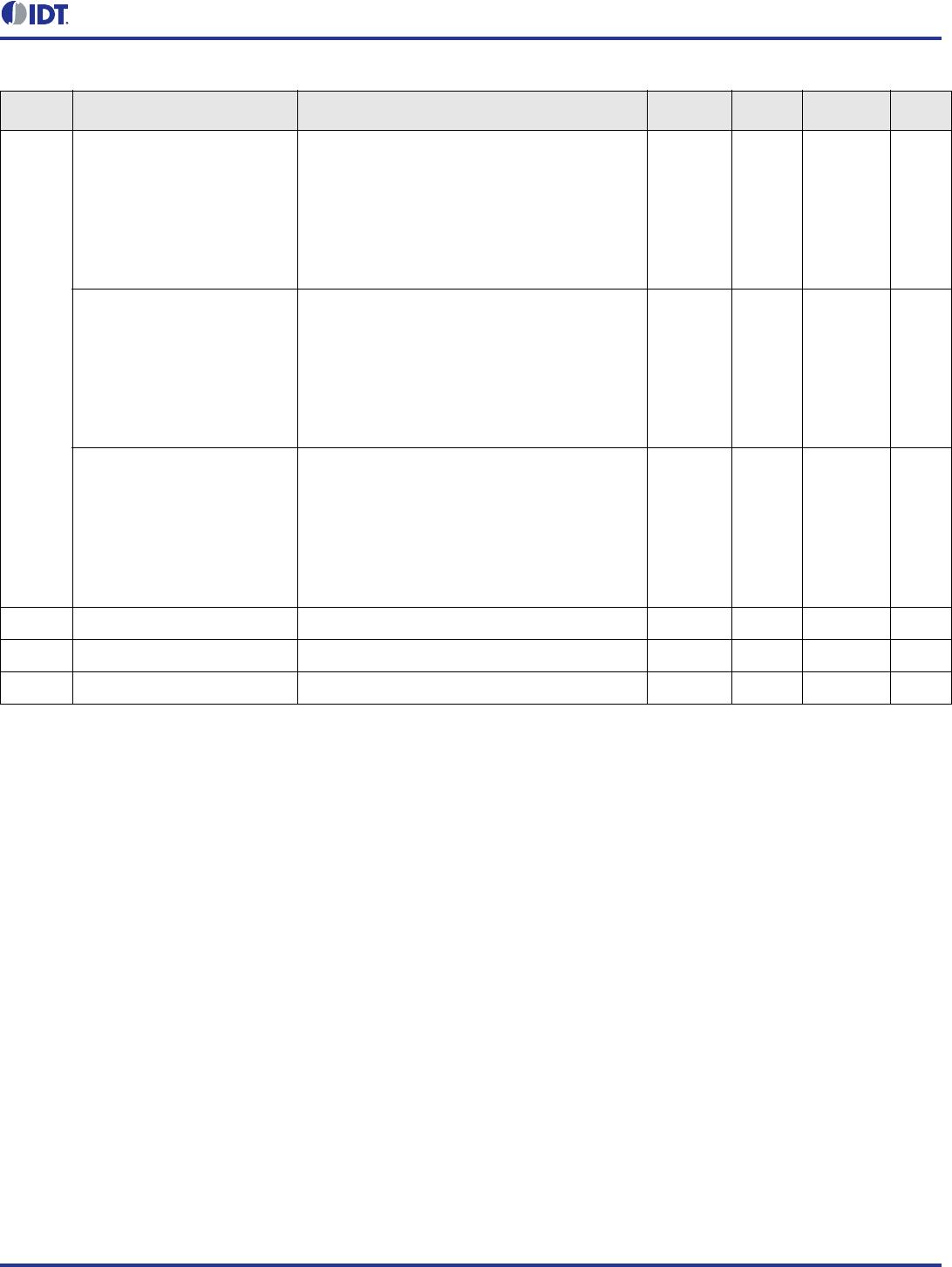
C Bus Characteristics
1
A device must internally provide a hold time of at least 300ns for the SDA signal (referred to the V
IH(MIN)
of the SCL signal) to bridge the undefined
region of the falling edge of SCL.
Spread Spectrum Generation Specifications
Table 20. I2C Bus DC Characteristics
Symbol Parameter Conditions Minimum Typical Maximum Units
V
IH
Input High Level 0.7 × V
DD1_8
V
V
IL
Input Low Level 0.3 × V
DD1_8
V
V
HYS
Hysteresis of Inputs 0.05 × V
DD1_8
V
I
IN
Input Leakage Current ±1 μA
V
OL
Output Low Voltage I
OL
= 3mA. 0.4 V
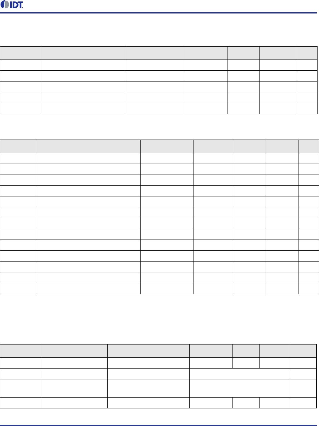
Table 21. I
2
C Bus AC Characteristics
Symbol Parameter Conditions Minimum Typical Maximum Units
F
SCLK
Serial Clock Frequency (SCL) 100 400 kHz
t
BUF
Bus Free-time between STOP and START 1.3 μs
t
SU:START
Setup Time, START 0.6 μs
t
HD:START
Hold Time, START 0.6 μs
t
SU:DATA
Setup Time, Data Input (SDA) 100 μs
t
HD:DATA
Hold Time, Data Input (SDA) 1 0 μs
t
OVD
Output Data Valid from Clock 0.9 μs
C
B
Capacitive Load for each Bus Line 400 pF
t
R
Rise Time, Data and Clock (SDA, SCL) 20 + 0.1 × C
B
300 ns
t
F
Fall Time, Data and Clock (SDA, SCL) 20 + 0.1 × C
B
300 ns
t
HIGH
High Time, Clock (SCL) 0.6 μs
t
LOW
Low Time, Clock (SCL) 1.3 μs
t
SU:STOP
Setup Time, STOP 0.6 μs
Table 22: Spread Spectrum Generation Specifications
Symbol Parameter Description Minimum Typical Maximum Units
f
OUT
Output Frequency Output frequency range. 1 125 MHz
f
MOD
Modulation Frequency Modulation frequency. 30 to 63 kHz
f
SPREAD
Spread Value
Amount of spread value
(programmable) – down spread.
-0.5% to -2% %f
OUT
% tolerance Spread% Value Variation of spread range. 15 %