22©2017 Integrated Device Technology, Inc. October 24, 2017
5L2503 Datasheet
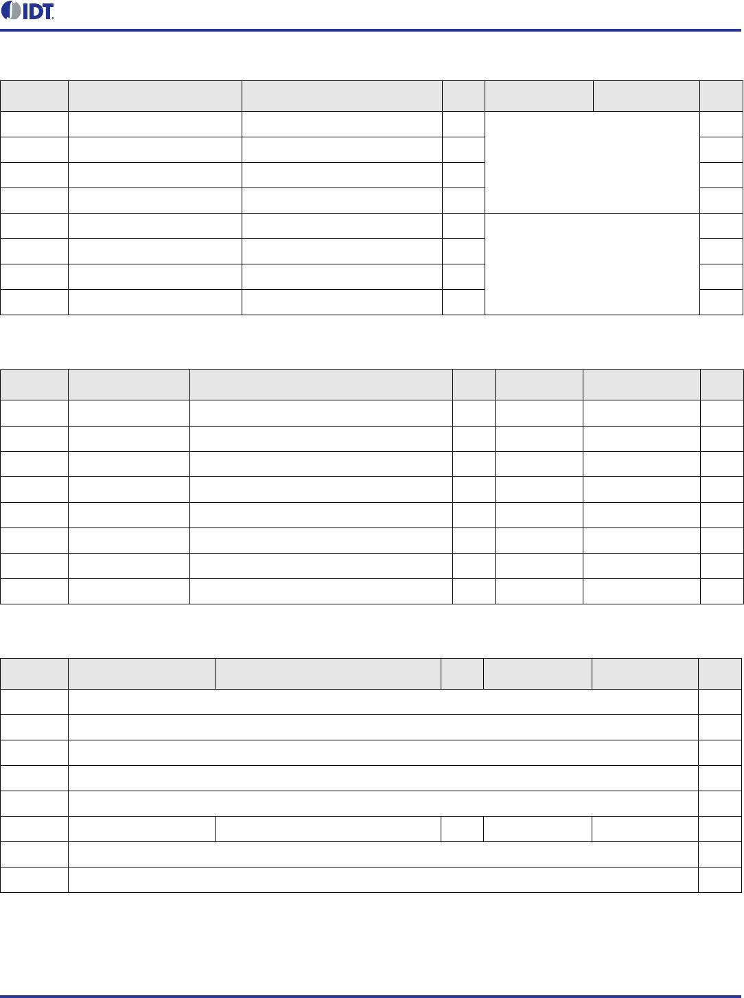
Byte 24: PLL2 Control Register
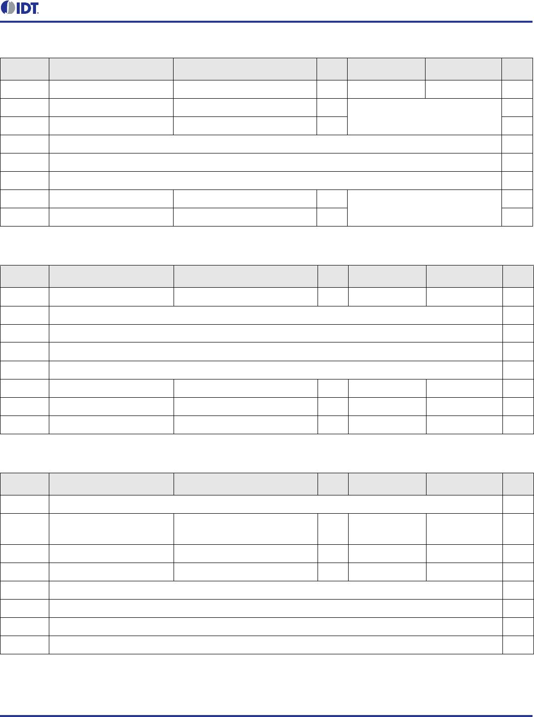
Byte 25: PLL2 Charge Pump Control
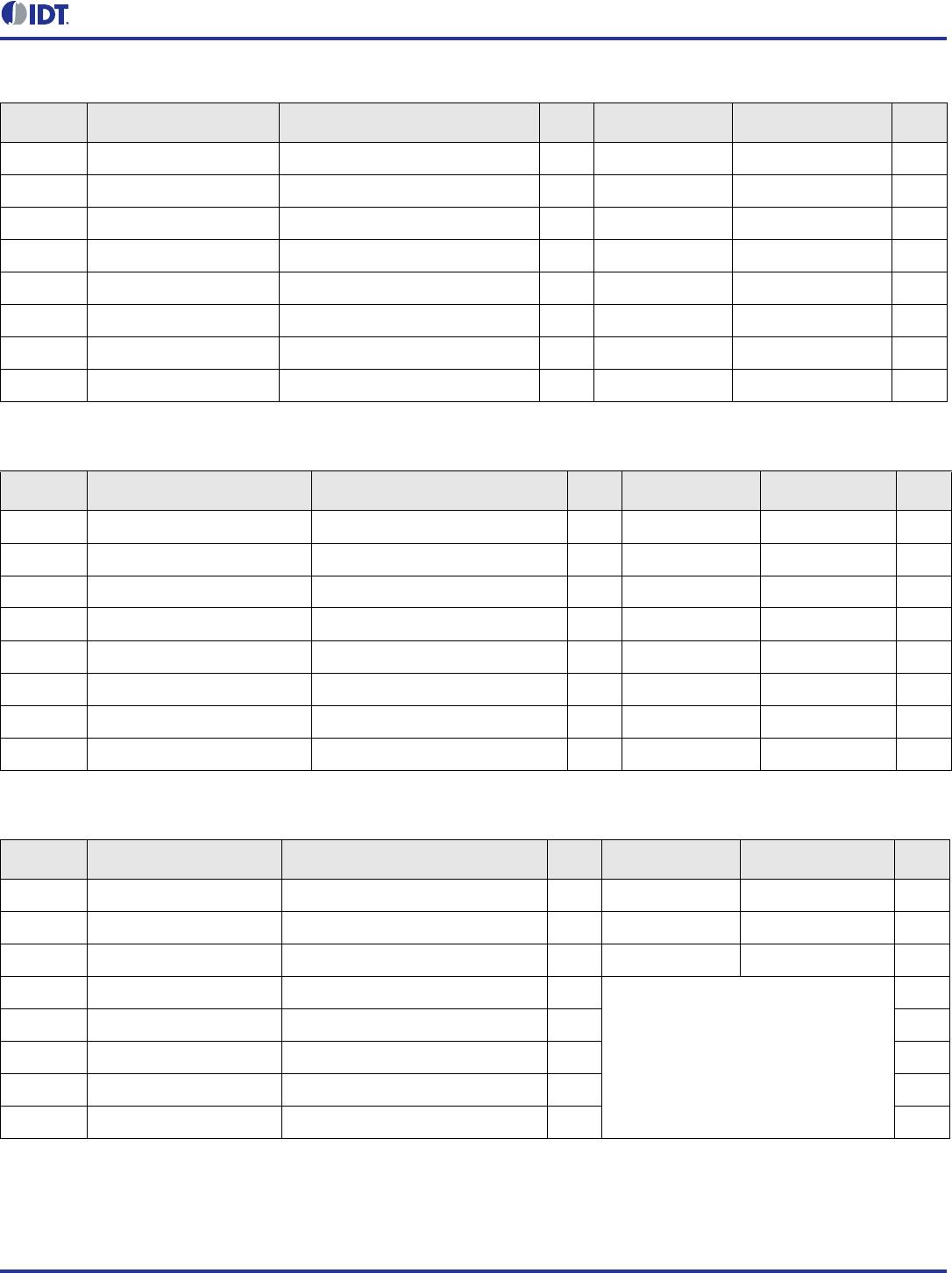
Byte 26: PLL2 M Divider Setting
Byte 18h Name Control Function Type 0 1 PWD
Bit 7 PLL2_PERIOD[9] PLL2 period control bit 9 R/W 0
Bit 6 PLL2_PERIOD[8] PLL2 period control bit 8 R/W 0
Bit 5 PLL2_SSEN PLL2 spread spectrum enable R/W disable enable 0
Bit 4 PLL2_R100K PLL2 loop filter resister 100kohm bypass plus 100kohm 0
Bit 3 PLL2_R50K PLL2 loop filter resister 50kohm bypass plus 50kohm 1
Bit 2 PLL2_R25K PLL2 loop filter resister 25kohm bypass plus 25kohm 1
Bit 1 PLL2_R12.5K PLL2 loop filter resister 12.5kohm bypass plus 12.5kohm 1
Bit 0 PLL2_R6K PLL2 loop filter resister 6kohm bypass only 6kohm applied 0
Byte 19h Name Control Function Type 0 1 PWD
Bit 7 PLL2_CP_16X PLL2 charge pump control R/W x16 0
Bit 6 PLL2_CP_8X PLL2 charge pump control R/W x8 0
Bit 5 PLL2_CP_4X PLL2 charge pump control R/W x4 0
Bit 4 PLL2_CP_2X PLL2 charge pump control R/W x2 1
Bit 3 PLL2_CP_1X PLL2 charge pump control R/W x1 0
Bit 2 PLL2_CP_/24 PLL2 charge pump control R/W /24 1
Bit 1 PLL2_CP_/3 PLL2 charge pump control R/W /3 0
Bit 0 PLL2_SIREF PLL2 SiRef current selection R/W 10μA20μA0
Byte 1Ah Name Control Function Type 0 1 PWD
Bit 7 PLL2_MDIV_Doubler PLL2 reference divider - doubler R/W disable enable 0
Bit 6 PLL2_MDIV1 PLL2 reference divider 1 R/W disable M DIV1 bypadd divider (/1) 0
Bit 5 PLL2_MDIV2 PLL2 reference divider 2 R/W disable M DIV2 bypadd divider (/2) 0
Bit 4 PLL2_MDIV[4] PLL2 reference divider control bit 4 R/W
3–64, default is 26
1
Bit 3 PLL2_MDIV[3] PLL2 reference divider control bit 3 R/W 1
Bit 2 PLL2_MDIV[2] PLL2 reference divider control bit 2 R/W 0
Bit 1 PLL2_MDIV[1] PLL2 reference divider control bit 1 R/W 1
Bit 0 PLL2_MDIV[0] PLL2 reference divider control bit 0 R/W 0
23©2017 Integrated Device Technology, Inc. October 24, 2017
5L2503 Datasheet
Byte 27: Output Divider 4
Byte 28: PLL Operation Control Register
Byte 29: Output Control
Byte 1Bh Name Control Function Type 0 1 PWD
Bit 7 OUTDIV3[3] Out divider 4 control bit 7 R/W
DIV3[3:2] = 1,2,4,5; DIV3[1:0] =
1,3,5,10; Default Divider = 1 x 5 = 5
0
Bit 6 OUTDIV3[2] Out divider 4 control bit 6 R/W 0
Bit 5 OUTDIV3[1] Out divider 4 control bit 5 R/W 1
Bit 4 OUTDIV3[0] Out divider 4 control bit 4 R/W 0
Bit 3 OUTDIV4[3] Out divider 4 control bit 3 R/W
DIV4[3:2] = 1,2,4,8; DIV4[1:0] =
1,3,5,10; Default Divider = 1 x 10 =
10
0
Bit 2 OUTDIV4[2] Out divider 4 control bit 2 R/W 0
Bit 1 OUTDIV4[1] Out divider 4 control bit 1 R/W 1
Bit 0 OUTDIV4[0] Out divider 4 control bit 0 R/W 1
Byte 1Ch Name Control Function Type 0 1 PWD
Bit 7 PLL2_HRS_EN PLL2 spread high resolution selection enable R/W normal enable (shift 4 bits) 0
Bit 6 PLL2_refin_sel PLL2 reference clock source select R/W Xtal DIV2 0
Bit 5 PLL3_PDB PLL3 power down R/W power down running 0
Bit 4 PLL3_LCKBYPSSB PLL3 lock bypass R/W bypass lock lock 0
Bit 3 PLL2_PDB PLL2 power down R/W power down running 1
Bit 2 PLL2_LCKBYPSSB PLL2 lock bypass R/W bypass lock lock 1
Bit 1 PLL1_PDB PLL1 power down R/W power down running 0
Bit 0 PLL1_LCKBYPSSB PLL1 lock bypass R/W bypass lock lock 0
Byte 1Dh Name Control Function Type 0 1 PWD
Bit 7 Reserved 0
Bit 6 Reserved 0
Bit 5 Reserved 1
Bit 4 Reserved 1
Bit 3 Reserved 0
Bit 2 VDD1_SEL VDD1_SEL R/W 1.8V 1.2V 0
Bit 1 Reserved 0
Bit 0 Reserved 0
24©2017 Integrated Device Technology, Inc. October 24, 2017
5L2503 Datasheet
Byte 30: OE and DFC Control
Byte 31: Control Register
Byte 32: Control Register
Byte 1Eh Name Control Function Type 0 1 PWD
Bit 7 OUT1_EN OUT1 output enable control R/W disable enable 1
Bit 6 OE1_fun_sel[1] OE1 pin function selection bit 1 R/W
11:DFC0 10: OUT_PPS
01: PD# 00: OUT1 OE
0
Bit 5 OE1_fun_sel[0] OE1 pin function selection bit 0 R/W 0
Bit 4 Reserved 1
Bit 3 Reserved 1
Bit 2 Reserved 0
Bit 1 DFC_SW_Sel[1] DFC frequency select bit 1 R/W
00: N0 01: N1 10:N2 11:N3
0
Bit 0 DFC_SW_Sel[0] DFC frequency select bit 0 R/W 0
Byte 1Fh Name Control Function Type 0 1 PWD
Bit 7 OUT2 free run_b OUT2 free run_b R/W freerun stoppable 1
Bit 6 Reserved 0
Bit 5 Reserved 0
Bit 4 Reserved 0
Bit 3 Reserved 0
Bit 2 PLL2_3rd_EN_CFG PLL2 3rd order control R/W 1st order 3rd order 1
Bit 1 OUTDIV5 source OUTDIV5 source R/W PLL3 DIV4seed 0
Bit 0 PLL2_EN_3rdpole PLL2 3rd pole control R/W disable enable 0
Byte 20h Name Control Function Type 0 1 PWD
Bit 7 Reserved 1
Bit 6 OUT2_fun_sel OUT2 pin function selection R/W
OE1pin
controlled
OE1pin not
controlled
1
Bit 5 Reserved 0
Bit 4 DFC_EN DFC function control R/W disable enable 0
Bit 3 Reserved 0
Bit 2 Reserved 0
Bit 1 Reserved 0
Bit 0 Reserved 0

5L2503-000NVGI

Mfr. #:
Manufacturer:
IDT
Description:
Clock Generators & Support Products Microclock Programmable Clock Generator
Lifecycle:
New from this manufacturer.
Delivery:
DHL FedEx Ups TNT EMS
Payment:
T/T Paypal Visa MoneyGram Western Union

Products related to this Datasheet