13©2017 Integrated Device Technology, Inc. October 24, 2017
5L2503 Datasheet
General I
2
C Serial Interface Information
How to Write
Controller (host) sends a start bit
Controller (host) sends the write address
IDT clock will acknowledge
Controller (host) sends the beginning byte location = N
IDT clock will acknowledge
Controller (host) sends the byte count = X
IDT clock will acknowledge
Controller (host) starts sending Byte N through Byte N+X-1
IDT clock will acknowledge each byte one at a time
Controller (host) sends a stop bit
How to Read
Controller (host) will send a start bit
Controller (host) sends the write address
IDT clock will acknowledge
Controller (host) sends the beginning byte location = N
IDT clock will acknowledge
Controller (host) will send a separate start bit
Controller (host) sends the read address
IDT clock will acknowledge
IDT clock will send the data byte count = X
IDT clock sends Byte N+X-1
IDT clock sends Byte 0 through Byte X (if X
(H)
was written to
Byte 8)
Controller (host) will need to acknowledge each byte
Controller (host) will send a not acknowledge bit
Controller (host) will send a stop bit
Index Block Write Operation
Controller (Host) IDT (Slave/Receiver)
T starT bit
Slave Address
WR WRite
ACK
Beginning Byte = N
ACK
Data Byte Count = X
ACK
Beginning Byte N
X Byte
ACK
O
OO
OO
O
Byte N + X - 1
ACK
PstoP bit
Index Block Read Operation
Controller (Host) IDT (Slave/Receiver)
TstarT bit
Slave Address
WR WRite
ACK
Beginning Byte = N
ACK
RT Repeat starT
Slave Address
RD ReaD
ACK
Data Byte Count=X
ACK
X Byte
Beginning Byte N
ACK
O
OO
OO
O
Byte N + X - 1
N Not acknowledge
PstoP bit
14©2017 Integrated Device Technology, Inc. October 24, 2017
5L2503 Datasheet
Byte 0: General Control
Byte 1: Dash Code ID (optional)
Byte 2: Crystal Cap Setting
Byte 00h Name Control Function Type 0 1 PWD
Bit 7 OTP_Burned
OTP memory programming
indication
R/W
OTP memory
non-programmed
OTP memory
programmed
0
Bit 6 I2C_addr[1] I
2
C address select bit 1 R/W
00: D0 / 01: D2
10: D4 / 11: D6
0
Bit 5 I2C_addr[0] I
2
C address select bit 0 R/W 0
Bit 4 PLL1_SSEN PLL1 Spread Spectrum enable R/W disable enable 0
Bit 3 Reserved 0
Bit 2 PLL3_refin_sel PLL3 source selection R/W Xtal Seed (DIV2) 0
Bit 1 Reserved 0
Bit 0 OTP_protect OTP memory protection R/W read/write write locked 0
Byte 01h Name Control Function Type 0 1 PWD
Bit 7 DashCode ID[7] Dash code ID R/W 0
Bit 6 DashCode ID[6] Dash code ID R/W 0
Bit 5 DashCode ID[5] Dash code ID R/W 0
Bit 4 DashCode ID[4] Dash code ID R/W 0
Bit 3 DashCode ID[3] Dash code ID R/W 0
Bit 2 DashCode ID[2] Dash code ID R/W 0
Bit 1 DashCode ID[1] Dash code ID R/W 0
Bit 0 DashCode ID[0] Dash code ID R/W 0
Byte 02h Name Control Function Type 0 1 PWD
Bit 7 Reserved 0
Bit 6 Reserved 0
Bit 5 Reserved 0
Bit 4 Reserved 1
Bit 3 Reserved 0
Bit 2 Reserved 0
Bit 1 Reserved 0
Bit 0 Reserved 0
15©2017 Integrated Device Technology, Inc. October 24, 2017
5L2503 Datasheet
Byte 3: PLL3 M Divider
Byte 4: PLL3 N Divider
Byte 5: PLL3 Loop Filter Setting and N Divider 10:8
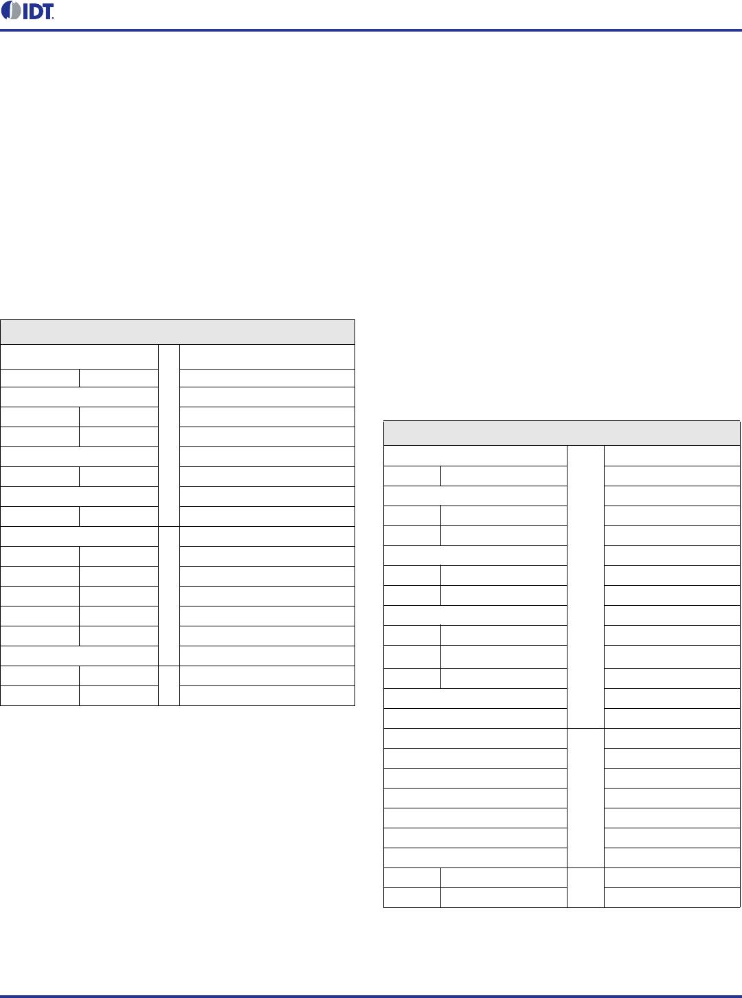
Byte 03h Name Control Function Type 0 1 PWD
Bit 7 PLL3_MDIV1 PLL3 source clock divider R/W disable M DIV1 bypadd divider (/1) 0
Bit 6 PLL3_MDIV2 PLL3 source clock divider R/W disable M DIV2 bypadd divider (/2) 0
Bit 5 PLL3 M_DIV[5] PLL3 reference integer divider R/W
3–64, default 26
0
Bit 4 PLL3 M_DIV[4] PLL3 reference integer divider R/W 1
Bit 3 PLL3 M_DIV[3] PLL3 reference integer divider R/W 1
Bit 2 PLL3 M_DIV[2] PLL3 reference integer divider R/W 0
Bit 1 PLL3 M_DIV[1] PLL3 reference integer divider R/W 1
Bit 0 PLL3 M_DIV[0] PLL3 reference integer divider R/W 0
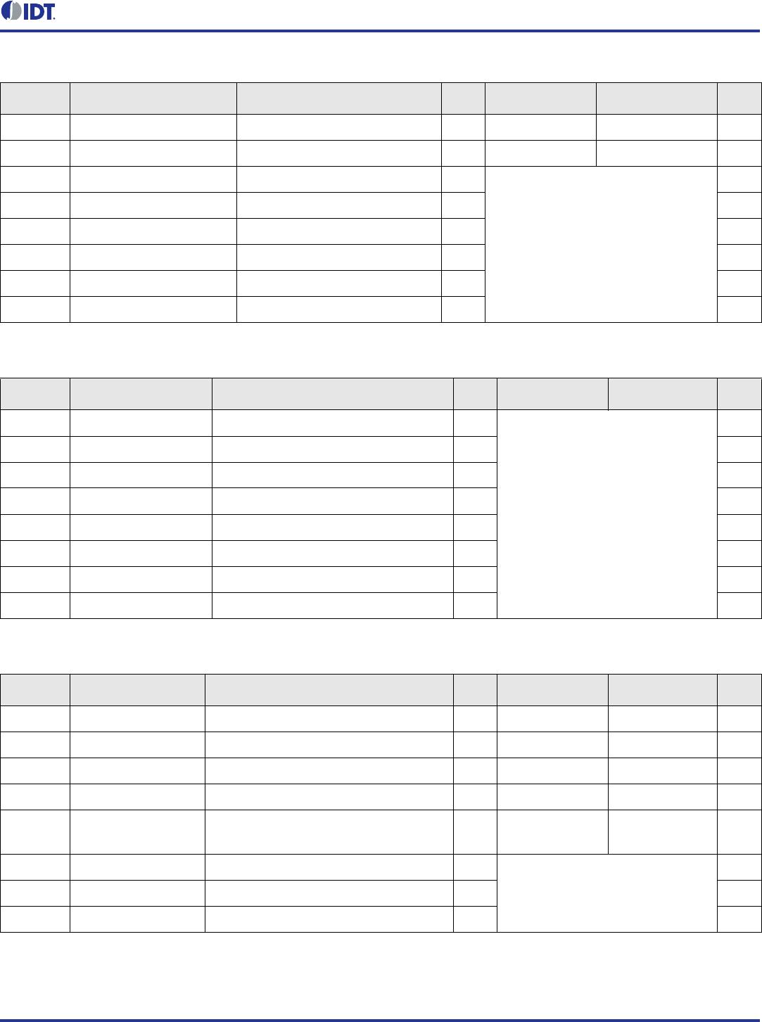
Byte 04h Name Control Function Type 0 1 PWD
Bit 7 PLL3 N_DIV[7] PLL3 VCO feedback integer divider bit7 R/W
12–2048, default VCO setting is
480MHz
1
Bit 6 PLL3 N_DIV[6] PLL3 VCO feedback integer divider bit6 R/W 1
Bit 5 PLL3 N_DIV[5] PLL3 VCO feedback integer divider bit5 R/W 1
Bit 4 PLL3 N_DIV[4] PLL3 VCO feedback integer divider bit4 R/W 0
Bit 3 PLL3 N_DIV[3] PLL3 VCO feedback integer divider bit3 R/W 0
Bit 2 PLL3 N_DIV[2] PLL3 VCO feedback integer divider bit2 R/W 0
Bit 1 PLL3 N_DIV[1] PLL3 VCO feedback integer divider bit1 R/W 0
Bit 0 PLL3 N_DIV[0] PLL3 VCO feedback integer divider bit0 R/W 0
Byte 05h Name Control Function Type 0 1 PWD
Bit 7 PLL3_R100K PLL3 Loop filter resister 100kohm R/W bypass plus 100kohm 0
Bit 6 PLL3_R50K PLL3 Loop filter resister 50kohm R/W bypass plus 50kohm 0
Bit 5 PLL3_R25K PLL3 Loop filter resister 25kohm R/W bypass plus 25kohm 0
Bit 4 PLL3_R12.5K PLL3 Loop filter resister 12.5kohm R/W bypass plus 12.5kohm 1
Bit 3 PLL3_R6K PLL3 Loop filter resister 6kohm R/W bypass
only 6kohm
applied
0
Bit 2 PLL3 N_DIV[10] PLL3 VCO feedback integer divider bit10 R/W
12–2048, default VCO setting is
480MHz
0
Bit 1 PLL3 N_DIV[9] PLL3 VCO feedback integer divider bit9 R/W 0
Bit 0 PLL3 N_DIV[8] PLL3 VCO feedback integer divider bit8 R/W 1

5L2503-000NVGI

Mfr. #:
Manufacturer:
IDT
Description:
Clock Generators & Support Products Microclock Programmable Clock Generator
Lifecycle:
New from this manufacturer.
Delivery:
DHL FedEx Ups TNT EMS
Payment:
T/T Paypal Visa MoneyGram Western Union

Products related to this Datasheet