REV. B
AD7865
–9–
CONVERTER DETAILS
The AD7865 is a high speed, low power, four-channel simulta-
neous sampling 14-bit A/D converter that operates from a single
5 V supply. The part contains a 2.4 µs successive approximation
ADC, four track/hold amplifiers, an internal 2.5 V reference
and a high speed parallel interface. There are four analog inputs
which can be sampled simultaneously, thus preserving the
relative phase information of the signals on all four analog inputs.
Thereafter, conversions will be completed on the selected sub-
set of the four channels. The part accepts an analog input
range of ± 10 V or ±5 V (AD7865-1), 0 V to 2.5 V or 0 V to 5 V
(AD7865-2) and ± 2.5 V (AD7865-3). Overvoltage protection
on the analog inputs for the part allows the input voltage to go
to ± 18 V (AD7865-1 with ± 10 V input range), ±9 V (AD7865-1
with ± 5 V input range), –1 V to +18 V (AD7865-2) and –4 V to
+18 V (AD7865-3) without causing damage or effecting the con-
version result of another channel.
The AD7865 has two operating
modes Reading Between Conversions and Reading after the Con-
version Sequence. These modes are discussed in more detail in the
Timing and Control section.
A conversion is initiated on the AD7865 by pulsing the CONVST
input. On the rising edge of CONVST, all four on-chip track/
holds are simultaneously placed into hold and the conversion
sequence is started on all the selected channels. Channel selec-
tion is made via the SL1–SL4 pins if H/S SEL is logic zero, or
via the channel select register if H/S SEL is logic one—see
Selecting a Conversion Sequence. The channel select register is
programmed via the bidirectional data lines DB0–DB3 and a
standard write operation. The selected conversion sequence is
latched on the rising edge of CONVST so changing a selection
will only take effect once a new conversion sequence is initi-
ated. The BUSY output signal is triggered high on the rising
edge of CONVST and will remain high for the duration of the
conversion sequence. The conversion clock for the part is gen-
erated internally using a laser-trimmed clock oscillator circuit.
There is also the option of using an external clock, by tying the
INT/EXT CLK pin logic high and applying an external clock
to the CLKIN pin. However, the optimum throughput is obtained
by using the internally generated clock— see Using an External
Clock. The EOC signal indicates the end of each conversion in the
conversion sequence. The BUSY signal indicates the end of the
full conversion sequence and at this time all four Track and Holds
return to tracking mode. The conversion results can either be read
at the end of the full conversion sequence (indicated by BUSY
going low) or as each result becomes available (indicated by EOC
going low). Data is read from the part via a 14-bit parallel data bus
with standard CS and RD signals—see Timing and Control.
Conversion time for each channel of the AD7865 is 2.4 µs and
the track/hold acquisition time is 0.35 µs. To obtain optimum
performance from the part, the read operation should not occur
during a channel conversion or during the 100 ns prior to the
next CONVST rising edge. This allows the part to operate at
throughput rates up to 100 kHz for all four channels and achieve
data sheet specifications.
Track/Hold Section
The track/hold amplifiers on the AD7865 allows the ADCs to
accurately convert an input sine wave of full-scale amplitude to
14-bit accuracy. The input bandwidth of the track/hold is greater
than the Nyquist rate of the ADC even when the ADC is oper-
ated at its maximum throughput rate of 350 kSPS (i.e., the
track/hold can handle input frequencies in excess of 175 kHz).
The track/hold amplifiers acquire input signals to 14-bit accu-
racy in less than 350 ns. The operation of the track/holds are
essentially transparent to the user. The four track/hold amplifi-
ers sample their respective input channels simultaneously, on
the rising edge of CONVST. The aperture time for the track/
holds (i.e., the delay time between the external CONVST signal
and the track/hold actually going into hold) are typically 15 ns
and, more importantly, is well matched across the four track/
holds on one device and also well matched from device to device.
This allows the relative phase information between different
input channels to be accurately preserved. It also allows multiple
AD7865s to sample more than four channels simultaneously. At
the end of a conversion sequence, the part returns to its tracking
mode. The acquisition time of the track/hold amplifiers begins
at this point.
The autozero section of the track/hold circuit is designed to
work with input slew rates of up to 4 × π × (Full-Scale Span).
This corresponds to a full-scale sine wave of up to 4 MHz for
any input range. Slew rates above this level within the acquisi-
tion time may cause an incorrect conversion result to be returned
from the AD7865.
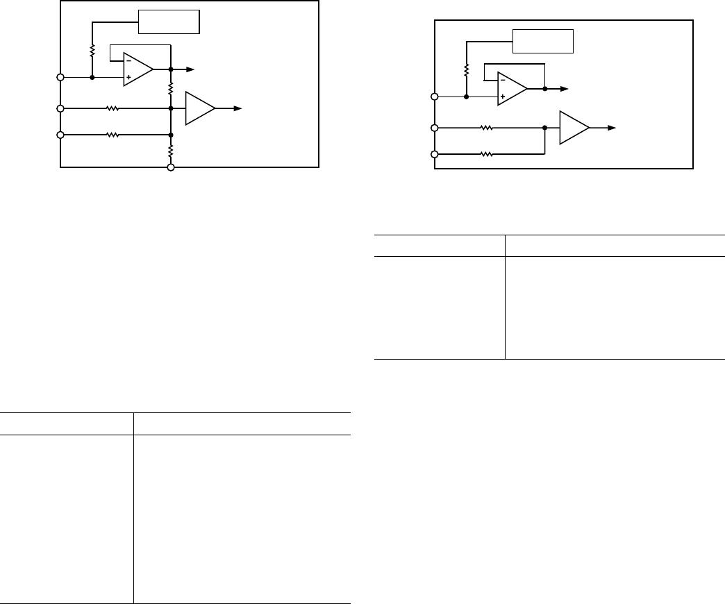
Reference Section
The AD7865 contains a single reference pin, labelled
V
REF
,
which either provides access to the part’s own 2.5 V reference or
allows an external 2.5 V reference to be connected to provide
the reference source for the part. The part is specified with a
2.5 V reference voltage.
The AD7865 contains an on-chip 2.5 V reference. To use this
reference as the reference source for the AD7865, simply con-
nect a 0.1 µF disc ceramic capacitor from the
V
REF
pin to AGND.
The voltage that appears at this pin is internally buffered before
being applied to the ADC. If this reference is required for use
external to the AD7865, it should be buffered as the part has a
FET switch in series with the reference output, resulting in a
source impedance for this output of 6 kΩ nominal. The toler-
ance on the internal reference is ± 10 mV at 25°C with a typical
temperature coefficient of 25 ppm/°C and a maximum error
over temperature of ±20 mV.
If the application requires a reference with a tighter tolerance or
the AD7865 needs to be used with a system reference, the user
has the option of connecting an external reference to this
V
REF
pin. The external reference will effectively overdrive the internal
reference and thus provide the reference source for the ADC.
The reference input is buffered before being applied to the ADC
with the maximum input current of ± 100 µA. Suitable reference
sources for the AD7865 include the AD680, AD780, REF192
and REF43 precision 2.5 V references.