REV. B
AD7865
–15–
When operating the AD7865 in a standby mode between con-
versions, the power savings can be significant. For example,
with a throughput rate of 10 kSPS and external reference, the
AD7865 will be powered up 11 µs out of every 100 µs (1 µs for
wake-up time and 9.6 µs to convert four channels. Therefore,
the average power consumption drops to (115 mW × 10.6%) or
12.2 mW approximately.
OFFSET AND FULL-SCALE ADJUSTMENT
In most Digital Signal Processing (DSP) applications, offset and
full-scale errors have little or no effect on system performance.
Offset error can always be eliminated in the analog domain by
ac coupling. Full-scale error effect is linear and does not cause
problems as long as the input signal is within the full dynamic
range of the ADC. Invariably, some applications will require
that the input signal span the full analog input dynamic range.
In such applications, offset and full-scale error will have to be
adjusted to zero.
Figure 13 shows a typical circuit that can be used to adjust the
offset and full-scale errors on the AD7865 (V
1
on the AD7865-1
version is shown for example purposes only). Where adjustment
is required, offset error must be adjusted before full-scale error.
This is achieved by trimming the offset of the op amp driving
the analog input of the AD7865 while the input voltage is
1/2 LSB below analog ground. The trim procedure is as follows:
apply a voltage of 610 µV (1/2 LSB) at V
1
and adjust the op
amp offset voltage until the ADC output code flickers between
1111 1111 1111 and 0000 0000 0000.
Gain error can be adjusted at either the first code transition
(ADC negative full scale) or the last code transition (ADC posi-
tive full scale). The trim procedures for both cases are as follows.
V
1
R1
10k
R2
500
R3
10k
AGND
AD7865*
*ADDITIONAL PINS OMITTED FOR CLARITY
INPUT
RANGE = 10V
R5
10k
V
INxA
R4
10k
Figure 13. Full-Scale Adjust Circuit
Positive Full-Scale Adjust
Apply a voltage of 9.9982 V (FS/2 3/2 LSB) at V
1
. Adjust R2
until the ADC output code flickers between 01 1111 1111 1110
and 01 1111 1111 1111.
Negative Full-Scale Adjust
Apply a voltage of 9.9998 V (FS + 1/2 LSB) at V
1
and adjust
R2 until the ADC output code flickers between 10 0000 0000
0000 and 10 0000 0000 0001.
An alternative scheme for adjusting full-scale error in systems
that use an external reference is to adjust the voltage at the V
REF
pin until the full-scale error for any of the channels is adjusted
out. The good full-scale matching of the channels will ensure
small full-scale errors on the other channels.
DYNAMIC SPECIFICATIONS
The AD7865 is specified and 100% tested for dynamic perfor-
mance specifications as well as traditional dc specifications such
as Integral and Differential Nonlinearity. These ac specifications
are required for such signal processing applications as phased array
sonar, adaptive filters and spectrum analysis. These applications
require information on the ADCs effect on the spectral content
of the input signal. Hence, the parameters for which the AD7865
is specified include SNR, harmonic distortion, intermodulation
distortion and peak harmonics. These terms are discussed in
more detail in the following sections.
Signal-to-Noise Ratio (SNR)
SNR is the measured signal-to-noise ratio at the output of the
ADC. The signal is the rms magnitude of the fundamental.
Noise is the rms sum of all the nonfundamental signals up to
half the sampling frequency (f
S
/2) excluding dc. SNR is depen-
dent upon the number of quantization levels used in the digitization
process; the more levels, the smaller the quantization noise. The
theoretical signal to noise ratio for a sine wave input is given by
SNR = (6.02N + 1.76) dB (1)
where N is the number of bits.
Thus for an ideal 14-bit converter, SNR = 86.04 dB.
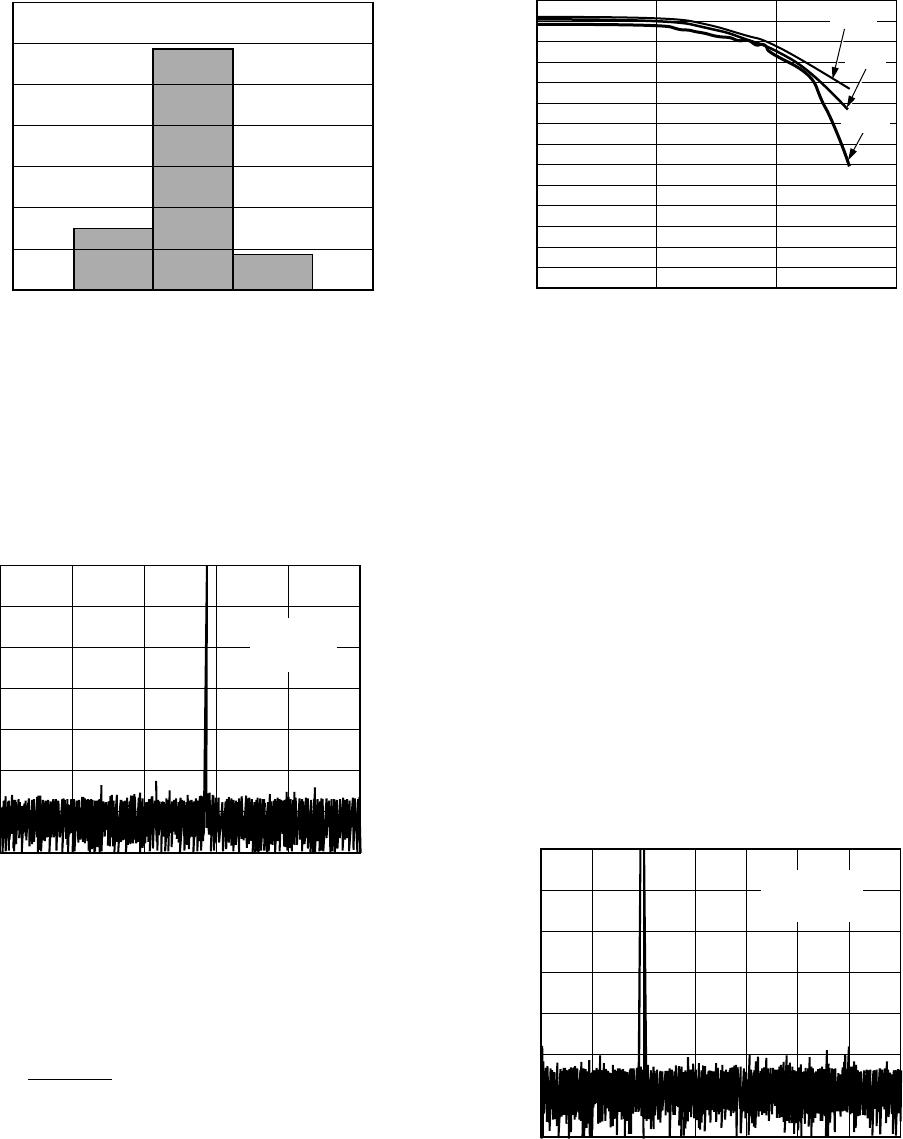
Figure 14 shows a histogram plot for 8192 conversions of a dc
input using the AD7865 with 5 V supply. The analog input was
set at the center of a code transition. It can be seen that most of
the codes appear in the one output bin, indicating very good
noise performance from the ADC.
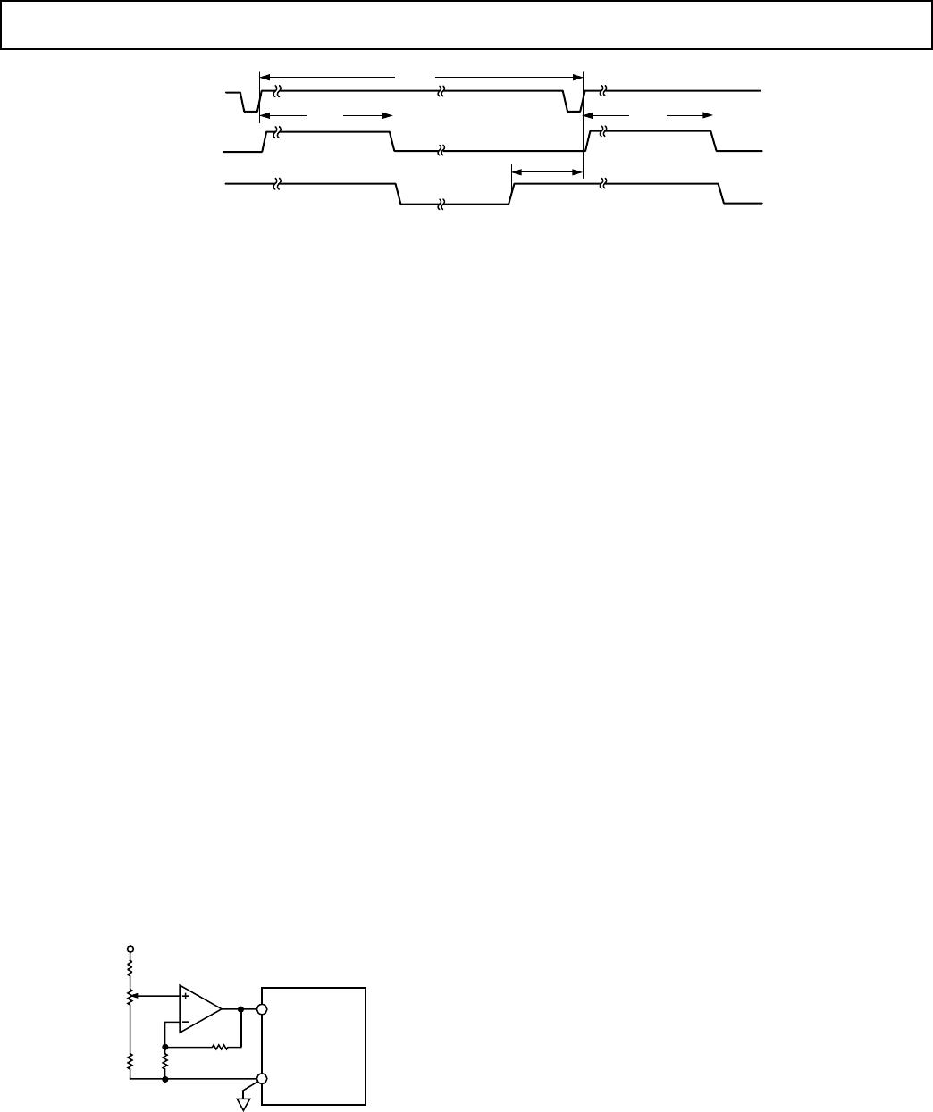
CONVST
BUSY
STBY
100s
I
DD
= 3A
t
BUSY
t
WAKEUP
t
BUSY
7s
Figure 12. Power-Down between Conversion Sequences
REV. B
AD7865
–16–
ADC CODE
7000
0
COUNTS
6000
5000
4000
3000
2000
1000
Figure 14. Histogram of 8192 Conversions of a DC Input
The output spectrum from the ADC is evaluated by applying a
sine wave signal of very low distortion to the analog input. A
Fast Fourier Transform (FFT) plot is generated from which the
SNR data can be obtained. Figure 15 shows a typical 4096-
point FFT plot of the AD7865 with an input signal of 100 kHz
and a sampling frequency of 350 kHz. The SNR obtained from
this graph is 80.5 dB. It should be noted that the harmonics are
taken into account when calculating the SNR.
FREQUENCY Hz
140
dBs
0 35000 70000
105000 140000 175000
f
s
= 350kHz
f
IN
= 100kHz
SNR = 80.5dB
120
100
80
60
40
20
0
Figure 15. FFT Plot
Effective Number of Bits
The formula given in Equation 1 relates the SNR to the number
of bits. Rewriting the formula, as in Equation 2, it is possible to
obtain a measure of performance expressed in effective number
of bits (N).
N
SNR
=
176
602
.
.
(2)
The effective number of bits for a device can be calculated
directly from its measured SNR. Figure 16 shows a typical plot
of effective number of bits versus frequency for an AD7865-2.
INPUT FREQUENCY kHz
0
ENOB
0
100
1000 10000
55C
+25C
1
2
3
4
5
6
7
8
9
10
11
12
13
14
+125C
Figure 16. Effective Numbers of Bits vs. Frequency
Intermodulation Distortion
With inputs consisting of sine waves at two frequencies, fa and
fb, any active device with nonlinearities will create distortion
products at sum and difference frequencies of mfa ± nfb where
m, n = 0, 1, 2, 3 . . ., etc. Intermodulation terms are those for
which neither m nor n are equal to zero. For example, the sec-
ond order terms include (fa + fb) and (fa fb) while the third
order terms include (2fa + fb), (2fa fb), (fa + 2fb) and (fa 2fb).
The AD7865 is tested using two input frequencies. In this case
the second and third order terms are of different significance.
The second order terms are usually distanced in frequency from
the original sine waves while the third order terms are usually at
a frequency close to the input frequencies. As a result, the second
and third order terms are specified separately. The calculation of
the intermodulation distortion is as per the THD specification
where it is the ratio of the rms sum of the individual distortion
products to the rms amplitude of the fundamental expressed in
dBs. In this case, the input consists of two, equal amplitude, low
distortion sine waves. Figure 17 shows a typical IMD plot for
the AD7865.
FREQUENCY Hz
0
140
dBs
0
25000 50000
100000 125000 175000
75000
150000
120
100
80
60
40
20
fa = 49.113kHz
f
b = 50.183kHz
f
s
= 350kHz
Figure 17. IMD Plot
REV. B
AD7865
–17–
AC Linearity Plots
The plots shown in Figure 18 below show typical DNL and INL
for the AD7865.
ADC Code
0
DNL LSBs
0.60
0 4000 8000 12000 16383
0.60
ADC Code
0
iNL LSBs
0.60
0 4000 8000 12000 16383
0.60
Figure 18. Typical DNL and INL Plots
MICROPROCESSOR INTERFACING
The high speed parallel interface of the AD7865 allows easy
interfacing to most DSPs and microprocessors. The AD7865
interface of the AD7865 consists of the data lines (DB0 to
DB13), CS, RD, WR, EOC and BUSY.
AD7865–ADSP-21xx Interface
Figure 19 shows an interface between the AD7865 and the
ADSP-210x. The CONVST signal can be generated by the
ADSP-210x or from some other external source. Figure 19
shows the CS being generated by a combination of the DMS
signal and the address bus of the ADSP-2100. In this way the
AD7865 is mapped into the data memory space of the
ADSP-210x.
The AD7865 BUSY line provides an interrupt to the ADSP-
210x when the conversion sequence is complete on all the
selected channels. The conversion results can then be read from
the AD7865 using successive read operations. Alternately, one
can use the EOC pulse to interrupt the ADSP-210x when the
conversion on each channel is complete when reading between
each conversion in the conversion sequence (Figure 8). The
AD7865 is read using the following instruction
MR0 = DM(ADC)
where MR0 is the ADSP-210x MR0 register and ADC is the
AD7865 address.
CS
RD
WR
BUSY
CONVST
DB0DB13
AD7865
V
IN1
V
IN2
V
IN3
V
IN4
DT1/F0
IRQn
RD
WR
D0D13
DMS
A0A13
ADSP-21xx
ADDRESS
DECODE
Figure 19. AD7865–ADSP-21xx Interface
AD7865–TMS320C5x Interface
Figure 20 shows an interface between the AD7865 and the
TMS320C5x. As with the previous interfaces, conversion can be
initiated from the TMS320C5x or from an external source and
the processor is interrupted when the conversion sequence is
completed. The CS signal to the AD7865 derived from the DS
signal and a decode of the address bus. This maps the AD7865
into external data memory. The RD signal from the TMS320 is
used to enable the ADC data onto the data bus. The AD7865
has a fast parallel bus so there are no wait state requirements.
The following instruction is used to read the conversion results
from the AD7865:
IN D,ADC
where D is Data Memory address and ADC is the AD7865
address.
PA0
INTn
DS
TMS320C5x
CS
RD
WR
BUSY
CONVST
DB0DB13
AD7865
V
IN1
V
IN2
V
IN3
V
IN4
RD
WR
D0D13
A0A13
ADDRESS
DECODE
Figure 20. AD7865–TMS320C5x Interface
AD7865–MC68000 Interface
An interface between the AD7865 and the MC68000 is shown
in Figure 21. The conversion can be initiated from the MC68000
or from an external source. The AD7865 BUSY line can be
used to interrupt the processor or, alternatively, software delays
can ensure that conversion has been completed before a read to
the AD7865 is attempted. Because of the nature of its inter-
rupts, the 68000 requires additional logic (not shown in Figure
21) to allow it to be interrupted correctly. For further informa-
tion on 68000 interrupts, consult the 68000 users manual.

AD7865ASZ-2REEL

Mfr. #:
Manufacturer:
Analog Devices Inc.
Description:
Analog to Digital Converters - ADC Fast Lo-Pwr 4-Ch Simult Sampling 14B
Lifecycle:
New from this manufacturer.
Delivery:
DHL FedEx Ups TNT EMS
Payment:
T/T Paypal Visa MoneyGram Western Union