REV. B
AD7865
–5–
CAUTION
ESD (electrostatic discharge) sensitive device. Electrostatic charges as high as 4000 V readily
accumulate on the human body and test equipment and can discharge without detection.
Although the AD7865 features proprietary ESD protection circuitry, permanent damage may
occur on devices subjected to high-energy electrostatic discharges. Therefore, proper ESD
precautions are recommended to avoid performance degradation or loss of functionality.
WARNING!
ESD SENSITIVE DEVICE
ABSOLUTE MAXIMUM RATINGS*
(T
A
= 25°C unless otherwise noted)
V
DD
to AGND . . . . . . . . . . . . . . . . . . . . . . . . . –0.3 V to +7 V
V
DD
to DGND . . . . . . . . . . . . . . . . . . . . . . . . . –0.3 V to +7 V
V
DRIVE
to DGND . . . . . . . . . . . . . . . . . . . . . . . . . V
DD
+ 0.3 V
Analog Input Voltage to AGND
AD7865-1 (± 10 V Input Range) . . . . . . . . . . . . . . . . ± 18 V
AD7865-1 (± 5 V Input Range) . . . . . . . . . . . . . . . . . . ± 9 V
AD7865-2 . . . . . . . . . . . . . . . . . . . . . . . . . . . –1 V to +18 V
AD7865-3 . . . . . . . . . . . . . . . . . . . . . . . . . . . –4 V to +18 V
Reference Input Voltage to AGND . . . –0.3 V to V
DD
+ 0.3 V
Digital Input Voltage to DGND . . . . . –0.3 V to V
DD
+ 0.3 V
Digital Output Voltage to DGND . . . . –0.3 V to V
DD
+ 0.3 V
Operating Temperature Range
Commercial (A, B Versions) . . . . . . . . . . . –40°C to +85°C
Automotive (Y Version) . . . . . . . . . . . . . . –40°C to +105°C
Storage Temperature Range . . . . . . . . . . . . –65°C to +150°C
Junction Temperature . . . . . . . . . . . . . . . . . . . . . . . . . 150°C
PQFP Package, Power Dissipation . . . . . . . . . . . . . . 450 mW
θ
JA
Thermal Impedance . . . . . . . . . . . . . . . . . . . . . 95°C/W
Lead Temperature, Soldering
Vapor Phase (60 sec) . . . . . . . . . . . . . . . . . . . . . . 215°C
Infrared (15 sec) . . . . . . . . . . . . . . . . . . . . . . . . . . 220°C
*Stresses above those listed under Absolute Maximum Ratings may cause perma-
nent damage to the device. This is a stress rating only; functional operation of the
device at these or any other conditions above those listed in the operational
sections of this specification is not implied. Exposure to absolute maximum rating
conditions for extended periods may affect device reliability.
ORDERING GUIDE
Input Relative Temperature Package Package
Model Ranges Accuracy Ranges Description Option
AD7865AS-1 ± 5 V, ±10 V ± 2 LSB –40°C to +85°C Plastic Lead Quad Flatpack S-44
AD7865BS-1 ± 5 V, ±10 V ± 1.5 LSB –40°C to +85°C Plastic Lead Quad Flatpack S-44
AD7865YS-1 ± 5 V, ±10 V ± 2 LSB –40°C to +105°C Plastic Lead Quad Flatpack S-44
AD7865AS-2 0 V to 2.5 V, 0 V to 5 V ± 2 LSB –40°C to +85°C Plastic Lead Quad Flatpack S-44
AD7865BS-2 0 V to 2.5 V, 0 V to 5 V ± 1.5 LSB –40°C to +85°C Plastic Lead Quad Flatpack S-44
AD7865YS-2 0 V to 2.5 V, 0 V to 5 V ± 2 LSB –40°C to +105°C Plastic Lead Quad Flatpack S-44
AD7865AS-3 ± 2.5 V ± 2 LSB –40°C to +85°C Plastic Lead Quad Flatpack S-44
AD7865BS-3 ± 2.5 V ± 1.5 LSB –40°C to +85°C Plastic Lead Quad Flatpack S-44
AD7865YS-3 ± 2.5 V ± 2 LSB –40°C to +105°C Plastic Lead Quad Flatpack S-44
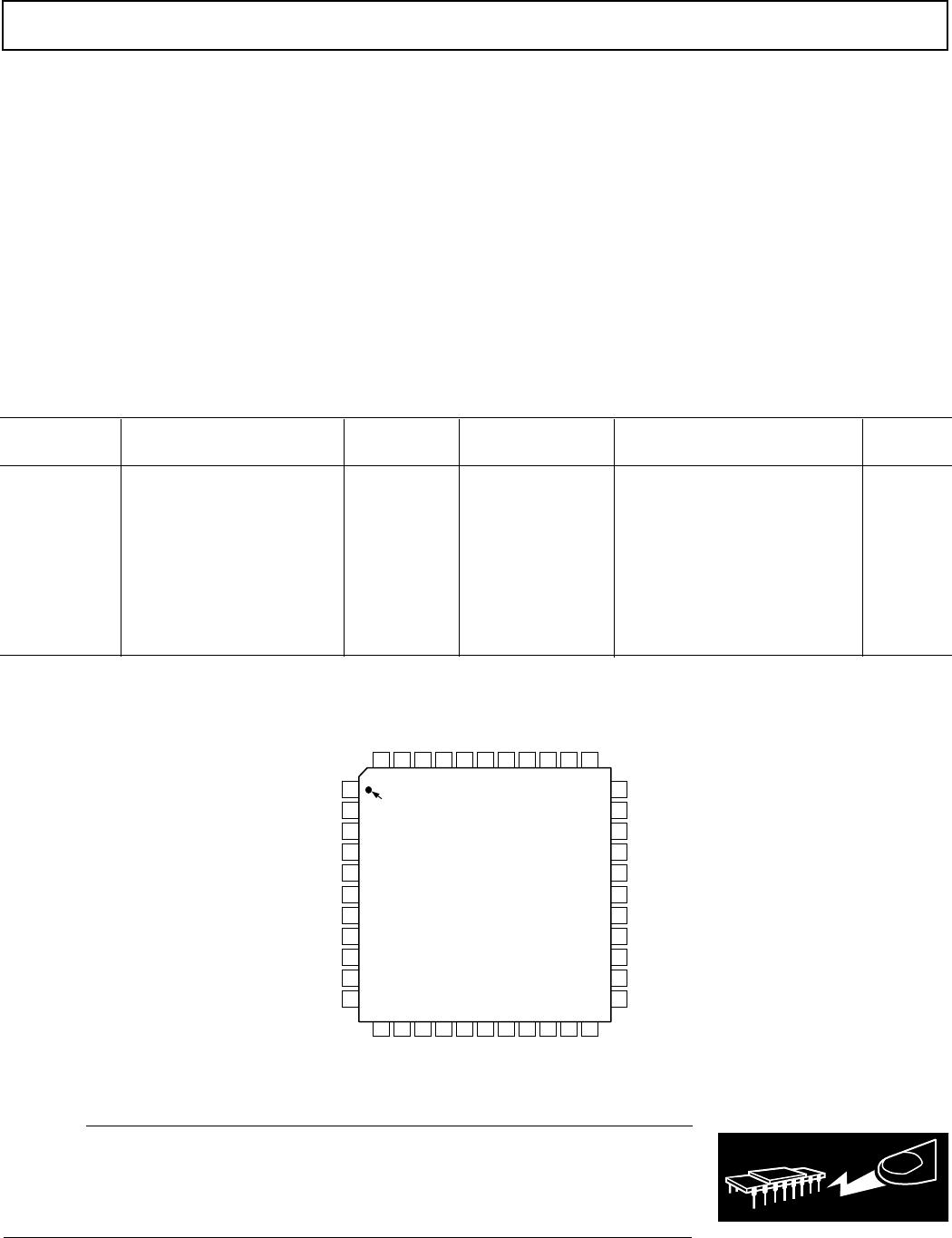
PIN CONFIGURATION
12 13 14 15 16 17 18 19
20
21 22
3
4
5
6
7
1
2
10
11
8
9
40 39 3841
42
4344 36 35 3437
PIN 1
IDENTIFIER
TOP VIEW
(Not to Scale)
29
30
31
32
27
28
25
26
23
24
33
DB7
DB8
DB0
DB1
DB2
DB3
DB4
DB5
DGND
V
DRIVE
DV
DD
DB6
EOC
DB9
DB10
DB12
DB13
AGND
AGND
AGND
V
I
N4B
V
IN4A
V
IN3B
V
IN3A
V
IN2B
BUSY
FRSTDATA
CONVST
CS
RD
WR
CLK IN/SL1
INT/EXT CLK/SL2
SL3
SL4
H/S SEL
AV
DD
V
REF
AGND
V
I
N2A
V
IN1B
V
I
N1A
STBY
AD7865
DB11