REV. B
AD7865
–13–
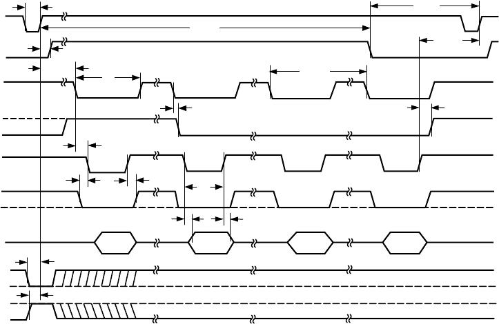
Accessing the Output Data Registers
There are four Output Data Registers, one for each of the four
possible conversion results from a conversion sequence. The
result of the first conversion in a conversion sequence is placed
in Register 1 and the second result is placed in Register 2 and so
on. For example if the conversion sequence V
IN1
, V
IN3
and V
IN4
is selected (see Selecting a Conversion Sequence) the results of
the conversion on V
IN1
, V
IN3
and V
IN4
are placed in Registers 1
to 3 respectively. The Output Data register pointer is reset to
point to Register 1 at the end of the first conversion in the
sequence, just prior to EOC going low. At this point the logic
output FRSTDATA will go logic high to indicate that the out-
put data register pointer is addressing Register 1. When CS and
RD are both logic low the contents of the addressed register are
enabled onto the data bus (DB0–DB13).
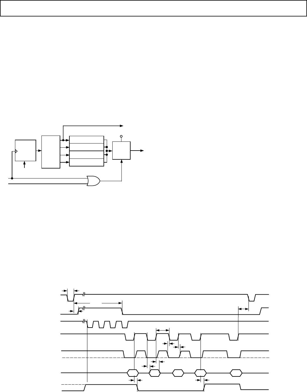
DB0 TO
DB13
O/P
DRIVERS
OE #1
NOT VALID
(V
IN3
)
(V
IN1
)
(V
IN4
)
OE #2
OE #3
OE #4
2-BIT
COUNTER
V
DRIVE
OE
RD
CS
RESET
OUTPUT
DATA REGISTERS
*THE POINTER WILL NOT BE INCREMENTED BY A RISING EDGE ON RD UNTIL
THE CONVERSION RESULT IS IN THE OUTPUT DATA REGISTER. THE POINTER
IS RESET WHEN THE LAST CONVERSION RESULT IS READ
FRSTDATA
POINTER*
AD7865
DECODE
Figure 8. Output Data Registers
When reading the output data registers after a conversion
sequence, i.e., when BUSY goes low, the register pointer is
incremented on the rising edge of the RD signal as shown in
Figure 8. However, when reading the conversion results between
conversions in a conversion sequence the pointer will not be
incremented until a valid conversion result is in the register to
be addressed. In this case the pointer is incremented when the
conversion has ended and the result has been transferred to the
output data register. This happens when EOC goes low, there-
fore EOC may be used to enable the register contents onto the
data bus as described in Reading Between Conversions in the
Conversion Sequence. The pointer is reset to point to Register 1
on the rising edge of the RD signal when the last conversion
result in the sequence is being read. In the example shown in
Figure 8, this means that the pointer is set to Register 1 when
the contents of Register 3 are read.
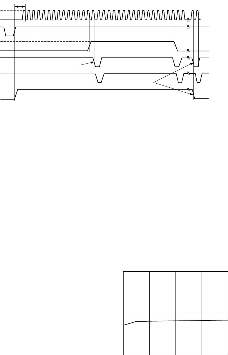
Reading after the Conversion Sequence
Figure 9 shows the same conversion sequence as Figure 7. In
this case, however, the results of the four conversions (on V
IN1
to V
IN4
) are read after all conversions have finished, i.e., when
BUSY goes logic low. The FRSTDATA signal goes logic high
at the end of the first conversion just prior to EOC going logic
low. As mentioned previously FRSTDATA has an indetermi-
nate state after initial power up, therefore FRSTDATA may
already be logic high. Unlike the case when reading during a
conversion the output data register pointer is incremented on
the rising edge of RD because the next conversion result is avail-
able in this case. This means FRSTDATA will go logic low after
the first rising edge on RD.
Successive read operations will access the remaining conversion
results in ascending channel order. Each read operation incre-
ments the output data register pointer. The read operation that
accesses the last conversion result causes the output data regis-
ter pointer to be reset so that the next read operation will access
the first conversion result again. This is shown in Figure 8 with
the fifth read after BUSY goes low accessing the result of the
conversion on V
IN1
. Thus the output data registers acts as a
circular buffer in which the conversion results may be continu-
ally accessed. The FRSTDATA signal will go high when the
first conversion result is available.
Data is enabled onto the data bus DB0 to DB13 using CS and
RD. Both CS and RD have the same functionality as described
in the previous section. There are no restrictions or performance
implications associated with the position of the read operations
after BUSY goes low, however there is a minimum time between
read operations that must be adhered to. Notice also that a “Quiet
Time” is needed before the start of the next conversion sequence.
t
10
t
8
t
4
t
3
t
6
t
1
QUIET
TIME
DATA
CONVST
BUSY
EOC
FRSTDATA
RD
CS
V
IN2
V
IN3
V
IN1
t
BUSY
t
2
t
10
t
7
V
IN1
V
IN4
Figure 9. Timing Diagram, Reading after the Conversion Sequences