General Description
The MAX16826 high-brightness LED (HB LED) driver is
designed for backlighting automotive LCD displays and
other display applications such as industrial or desktop
monitors and LCD televisions. The MAX16826 integrates
a switching regulator controller, a 4-channel linear cur-
rent sink driver, an analog-to-digital converter (ADC),
and an I
2
C interface. The IC is designed to withstand
automotive load dump transients up to 40V and can
operate under cold crank conditions.
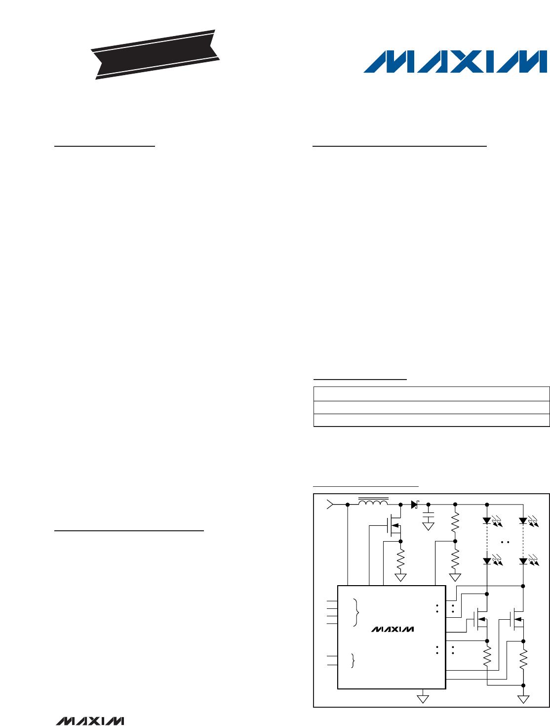
The MAX16826 contains a current-mode PWM switching
regulator controller that regulates the output voltage to
the LED array. The switching regulator section is config-
urable as a boost or SEPIC converter and its switching
frequency is programmable from 100kHz to 1MHz.
The MAX16826 includes 4 channels of programmable,
fault-protected, constant-current sink driver controllers
that are able to drive all white, RGB, or RGB plus amber
LED configurations. LED dimming control for each chan-
nel is implemented by direct PWM signals for each of the
four linear current sinks. An internal ADC measures the
drain voltage of the external driver transistors and the
output of the switching regulator. These measurements
are then made available through the I
2
C interface to an
external microcontroller (μC) to enable output voltage
optimization and fault monitoring of the LEDs.
The amplitude of the LED current in each linear current-
sink channel and the switch-mode regulator output volt-
age is programmed using the I
2
C interface. Additional
features include: cycle-by-cycle current limit, shorted
LED string protection, and overtemperature protection.
The MAX16826 is available in a thermally enhanced,
5mm x 5mm, 32-pin thin QFN package and is specified
over the automotive -40°C to +125°C temperature range.
Applications
LCD Backlighting:
Automotive Infotainment Displays
Automotive Cluster Displays
Industrial and Desktop Monitors
LCD TVs
Automotive Lighting:
Adaptive Front Lighting
Low- and High-Beam Assemblies
Features
o External MOSFETs Allow Wide-Range LED
Current with Multiple LEDs per String
o Individual PWM Dimming Inputs per String
o Very Wide Dimming Range
o LED String Short and Open Protection
o Adjustable LED Current Rise/Fall Times Improve
EMI Control
o Microcontroller Interface Using I
2
C Allows
LED Voltage Monitoring and Optimization
Using a 7-Bit Internal ADC
LED Short and Open Detection
Dynamic Adjustment of LED String Currents
and Output Voltage
Standby Mode
o Integrated Boost/SEPIC Controller
o External Switching Frequency Synchronization
o 4.75V to 24V Operating Voltage Range and
Withstands 40V Load Dump
o Overvoltage and Overtemperature Protection
MAX16826
Programmable, Four-String HB LED Driver with
Output-Voltage Optimization and Fault Detection
________________________________________________________________
Maxim Integrated Products
1
Ordering Information
19-4047; Rev 4; 12/11
For pricing, delivery, and ordering information, please contact Maxim Direct at 1-888-629-4642,
or visit Maxim’s website at www.maxim-ic.com.
EVALUATION KIT
AVAILABLE
PART TEMP RANGE PIN-PACKAGE
MAX16826ATJ+ - 40°C to + 125°C 32 TQFN-EP*
MAX16826ATJ/V+ - 40°C to + 125°C 32 TQFN-EP*
Typical Application Circuit and Pin Configuration appear at
end of data sheet.
+
Denotes a lead(Pb)-free/RoHS-compliant package.
*
EP = Exposed pad.
/V
denotes an automotive qualified part.
Simplified Diagram
MAX16826
DR4
DR1
DL1
IN
DL
BOOST LED DRIVER
CS FB
GND
V
IN
DIM1
DIM2
SDA
SCL
DIM3
DIM4
I
2
C
INTERFACE
DIMMING
INPUTS
CS1
DL4
CS4
Ordering Information continued at end of data sheet.
MAX16826
Programmable, Four-String HB LED Driver with
Output-Voltage Optimization and Fault Detection
2 _______________________________________________________________________________________
ABSOLUTE MAXIMUM RATINGS
ELECTRICAL CHARACTERISTICS
(V
IN
= 12V, R19 = 2kΩ, C33 = 2200pF, R17 = 1.27kΩ, C
DL_
= 0.01μF, T
J
= -40°C to +125°C, unless otherwise noted. Typical values
are at T
A
= +25°C.) (Note 1)
Stresses beyond those listed under “Absolute Maximum Ratings” may cause permanent damage to the device. These are stress ratings only, and functional
operation of the device at these or any other conditions beyond those indicated in the operational sections of the specifications is not implied. Exposure to
absolute maximum rating conditions for extended periods may affect device reliability.
IN to GND (Continuous) .........................................-0.3V to +30V
IN Peak Current ( 400ms) ...............................................300mA
IN Continuous Current ........................................................50mA
PGND to GND .......................................................-0.3V to +0.3V
All Other Pins to GND...............................................-0.3V to +6V
DL Peak Current (< 100ns)....................................................±3A
DL Continuous Current .....................................................±50mA
DL1, DL2, DL3, DL4 Peak Current ..................................±50mA
DL1, DL2, DL3, DL4 Continuous Current ........................±20mA
V
CC
Continuous Current .....................................................50mA
All Other Pins Current .......................................................±20mA
Continuous Power Dissipation (T
A
= +70°C)
32-Pin Thin QFN (derate 34.5mW/°C above +70°C)
Multilayer Board ..........................................................2759mW
Operating Temperature Range .........................-40°C to +125°C
Junction Temperature......................................................+150°C
Storage Temperature Range .............................-65°C to +150°C
Lead Temperature (soldering, 10s) ........…………………+300°C
Soldering Temperature (reflow) .......................................+260°C
PARAMETER SYMBOL CONDITIONS MIN TYP MAX UNITS
Power-Supply Voltage V
IN
V
SYNC
= 3V 4.75 24 V
Quiescent Current I
IN
DL_ = unconnected; R19, C33 = open 5 10 mA
Shutdown Current I
IN,SD
V
SYNC
= 0V 20 75 μA
Standby Current I
IN,SB
I
2
C standby activated 3 mA
I
2
C-COMPATIBLE I/O (SCL, SDA)
Input High Voltage V
IH
1.5 V
Input Low Voltage V
IL
0.5 V
Input Hysteresis V
HYS
25 mV
Input High Leakage Current I
IH
V
LOGIC
= 5V -1 +1 μA
Input Low Leakage Current I
IL
V
LOGIC
= 0V -1 +1 μA
Input Capacitance C
IN
10 pF
Output Low Voltage V
OL
I
OL
= 3mA 0.4 V
Output High Current I
OH
V
OH
= 5V 1 μA
I
2
C-COMPATIBLE TIMING
Serial Clock (SCL) Frequency f
SCL
400 kHz
BUS Free Time Between STOP
and START Conditions
t
BUF
1.3 μs
START Condition Hold Time t
HD:STA
0.6 μs
STOP Condition Setup Time t
SU:STO
0.6 μs
Clock Low Period t
LOW
1.3 μs
Clock High Period t
HIGH
0.6 μs
Data Setup Time t
SU:DAT
0.3 μs
Data In Hold Time t
HD:DATIN
0.03 0.9 μs
Data Out Hold Time t
HD:DATOUT
0.3 μs
MAX16826
Programmable, Four-String HB LED Driver with
Output-Voltage Optimization and Fault Detection
_______________________________________________________________________________________ 3
PARAMETER SYMBOL CONDITIONS MIN TYP MAX UNITS
Maximum Receive SCL/SDA Rise
Time
t
R
C
B
= 400pF 300 ns
Minimum Receive SCL/SDA Rise
Time
t
R
C
B
= 400pF 60 ns
Maximum Receive SCL/SDA Fall
Time
t
F
C
B
= 400pF 300 ns
Minimum Receive SCL/SDA Fall
Time
t
F
C
B
= 400pF 60 ns
Transmit SDA Fall Time t
F
C
B
= 400pF, I
O
= 3mA 60 250 ns
Pulse Width of Suppressed Spike t
SP
50 ns
INTERNAL REGULATORS (IN, V
CC
)
V
CC
Output Voltage V
VCC
0V < I
VCC
< 30mA (Note 2),
4.75V < V
IN
< 24V, DL, DL1 to DL4
unconnected
4.5 5.25 5.65 V
V
CC
Undervoltage Lockout V
VCC_UVLO
V
CC
rising 4.5 V
V
CC
Undervoltage Lockout
Hysteresis
V
VCC_HYS
135 175 205 mV
IN Shunt Regulation Voltage I
IN
= 250mA 24.05 26.0 27.5 V
PWM GATE DRIVER (DL)
Peak Source Current 2A
Peak Sink Current 2A
DL High-Side Driver Resistance I
DL
= -100mA 2.25 Ω
DL Low-Side Driver Resistance I
DL
= +100mA 1.30 Ω
Minimum DL Pulse Width 40 ns
PWM CONTROLLER, SOFT-START (FB, COMP, OVP)
FB shorted to COMP; MAX16826 only 1.230 1.250 1.260
FB Voltage Maximum V
FB,MAX
FB shorted to COMP; MAX16826B only 1.23 1.25 1.27
V
FB shorted to COMP; MAX16826 only 862 876 885
FB Voltage Minimum V
FB,MIN
FB shorted to COMP; MAX16826B only 735 750 765
mV
FB shorted to COMP; MAX16826 only 2.94
FB Voltage LSB
FB shorted to COMP; MAX16826B only 3.9
mV
FB Input Bias Current I
FB
0V < V
FB
< 5.5V -100 0 +100 nA
Feedback-Voltage Line
Regulation
Level to produce V
COMP
= 1.25V,
4.5V < V
VCC
< 5.5V
±0.25 %/V
Soft-Start Current I
SS
V
CSS
= 0.5V
VCC
3.2 6.0 10.4 μA
OVP Input Bias Current I
OVP
0V < V
OVP
< 5.5V -100 0 +100 nA
Slope Compensation I
SLOPE
19 26 32 μA/μs
ELECTRICAL CHARACTERISTICS (continued)
(V
IN
= 12V, R19 = 2kΩ, C33 = 2200pF, R17 = 1.27kΩ, C
DL_
= 0.01μF, T
J
= -40°C to +125°C, unless otherwise noted. Typical values
are at T
A
= +25°C.) (Note 1)

MAX16826ATJ+

Mfr. #:
Manufacturer:
Maxim Integrated
Description:
LED Lighting Drivers Prog 4-String HB
Lifecycle:
New from this manufacturer.
Delivery:
DHL FedEx Ups TNT EMS
Payment:
T/T Paypal Visa MoneyGram Western Union