Accessing the MAX16826
The communication between the μC and the MAX16826
is based on the usage of a set of protocols defined on
top of the standard I
2
C protocol definition. They are
exclusively write byte(s) and read byte(s).
Write Byte(s)
The write byte protocol is as follows:
1) The master sends a START condition.
2) The master sends the 7-bit slave address followed
by a write bit (low).
3) The addressed slave asserts an ACK by pulling
SDA low.
4) The master sends an 8-bit command code.
5) The slave asserts an ACK by pulling SDA low.
6) The master sends an 8-bit data byte.
7) The slave acknowledges the data byte.
8) The master generates a STOP condition or repeats
6 and 7 to write next byte(s).
The command is interpreted as the destination address
(register file unit) and data is written in the addressed
location. The slave asserts a NACK at step 5 if the com-
mand is not valid. The master then interrupts the com-
munication by issuing a STOP condition. If the address
is correct, the data byte is written to the addressed reg-
ister. After the write, the internal address pointer is
increased by one. When the last location is reached, it
cycles to the first register.
Read Byte(s)
The read sequence is:
1) The master sends a START condition.
2) The master sends the 7-bit slave address plus a
write bit (low).
3) The addressed slave asserts an ACK on the data
line.
4) The master sends an 8-bit command byte.
5) The active slave asserts an ACK on the data line.
6) The master sends a repeated START condition.
7) The master sends the 7-bit slave address plus a
read bit (high).
8) The addressed slave asserts an ACK on the data
line.
9) The slave sends an 8-bit data byte.
10) The master asserts a NACK on the data line to
complete operations or asserts an ACK and
repeats 9 and 10.
11) The master generates a STOP condition.
The data byte read from the device is the content of the
addressed location(s). Once the read is done, the inter-
nal pointer is increased by one. When the last location is
reached, it cycles to the first one. If the device is busy or
the address is not correct (out of memory map), the
command code is not acknowledged and the internal
address pointer is not altered. The master then inter-
rupts the communication by issuing a STOP condition.
MAX16826
Programmable, Four-String HB LED Driver with
Output-Voltage Optimization and Fault Detection
______________________________________________________________________________________ 19
S ACKSLAVE ADDRESS R/W
7 BITS 0
COMMAND
8 BITS
ACK ACK PDATA
COMMAND BYTE: SELECT REGISTER TO WRITE DATA BYTE DATA GOES INTO THE REGISTER
SET BY THE COMMAND BYTE
8 BITS
WRITE BYTE FORMAT
Figure 7. Write Byte Format
S ACKSLAVE ADDRESS R/W
7 BITS 0
ACKSLAVE ADDRESS R/W
7 BITS 1
COMMAND
8 BITS
ACK SR NACK PDATA
COMMAND BYTE: PREPARE DEVICE FOR
FOLLOWING READ
DATA BYTE DATA COMES FROM THE
REGISTER SET BY THE COMMAND BYTE
8 BITS
READ BYTE FORMAT
Figure 8. Read Byte Format
MAX16826
Register File Unit
The register file unit is used to store all the control infor-
mation from the SDA line and configure the MAX16826
for different operating conditions. The register file
assignments of the MAX16826 are in Table 2.
Registers 00h to 03h: String Current Programming
These registers are used to program LED string 1 to
LED string 4 current sink values. For each LED string,
CS1–CS4 inputs are connected to the source of the
external current sink FET and internally are connected
to the inverting input of the internal transconductance
amplifier. The noninverting input of this amplifier is con-
nected to the output of an internal DAC programmed
by these registers. As the DAC is incremented, its out-
put voltage decreases from 316mV to 97mV in 1.72mV
steps by the data written in the register 00h to 03h;
thus, the steady-state voltage at CS1–CS4 is given by
the following formula:
V
CS1,2,3,4
= 316mV - (1.72mV x RegisterValue[6:0])
For example, if 00h is set to 20h, then the CS1 voltage is:
V
CS1
= 316mV - 1.72mV x 32 = 265.3mV
Register 04h: Switching Regulator
Output Programming
Set the switching regulator output voltage by connect-
ing FB to the center of a resistive voltage-divider
between the switching regulator output and GND. V
FB
is regulated to a voltage from 876mV to 1.25V (typ) set
by the register 04h through the I
2
C interface.
The FB reference voltage can be decreased from 1.25V,
its maximum value, by approximately 2.9mV steps. The
steady-state voltage at FB then is regulated to:
V
FB
= 1.25V - (2.91mV x 04h[6:0])
Registers 05h to 08h: External Current-Sink
FET Drain Voltage ADC Readings
These registers store the drain voltages of the external
current sink FETs. For each register, bits 6–0 are the
conversion data of the ADC outputs. Bit 7 is used to
show if the conversion is terminated by the ADC (indi-
cated by 0) or if there is an internal timeout (indicated
by 1). If the drain voltage exceeds the preset reference
voltage, the corresponding LED string fault bit is assert-
ed. See the
Faults and Fault Detection
section for more
information on the internal timeout function.
Register 09h: Switching Regulator
Voltage ADC Output
Bits 6-0 of this register store the voltage present at
OVP. This voltage is a scaled down version of the
switching regulator output voltage. Bit 7 is not used.
Register 0Ah: Fault Status Register
This register stores all the external events or fault infor-
mation such as overvoltage and shorted LED string
faults. The fault events are logged only if the system is
not in standby mode and their active states are longer
than one clock cycle. Cycle enable or power to clear the
fault status register. Initiating standby mode using the
I
2
C interface can also be used to clear the fault status
Programmable, Four-String HB LED Driver with
Output-Voltage Optimization and Fault Detection
20 ______________________________________________________________________________________
Table 2. Register File Assignments
REGISTER
ADDRESS
R/W
USED BIT
RANGE
RESET
VALUE
DESCRIPTION
00h R/W [6:0] 00h LED String 1 current programming value.
01h R/W [6:0] 00h LED String 2 current programming value.
02h R/W [6:0] 00h LED String 3 current programming value.
03h R/W [6:0] 00h LED String 4 current programming value.
04h R/W [6:0] 00h Switching regulator output voltage programming value.
05h R [7:0] 00h LED String 1 external FET drain voltage ADC output.
06h R [7:0] 00h LED String 2 external FET drain voltage ADC output.
07h R [7:0] 00h LED String 3 external FET drain voltage ADC output.
08h R [7:0] 00h LED String 4 external FET drain voltage ADC output.
09h R [6:0] 00h OVP voltage, ADC output.
0Ah R [5:0] 00h Fault status register.
0Bh R/W [0] 00h Device standby command.
0Ch R [2:0] Device revision code.
register. First, activate standby mode and then deacti-
vate this mode using the I
2
C interface. Next, perform a
read operation on the fault status register. The old fault
information is reported in this first read operation. The
conclusion of the read operation clears the data con-
tained in the register. Subsequent read operations con-
firm that the fault status register has been cleared.
The description of this register is as follows:
Bit 0: Overvoltage sense flag. This flag is set if the volt-
age at OVP exceeds 1.25V; switching stops until power
or the enable or standby is cycled.
Bit 1: Not used.
Bit 2: LED string 1 shorted flag. A diode short in LED
string 1 has been detected if this bit is set.
Bit 3: LED string 2 shorted flag. A diode short in LED
string 2 has been detected if this bit is set.
Bit 4: LED string 3 shorted flag. A diode short in LED
string 3 has been detected if this bit is set.
Bit 5: LED string 4 shorted flag. A diode short in LED
string 4 has been detected if this bit is set.
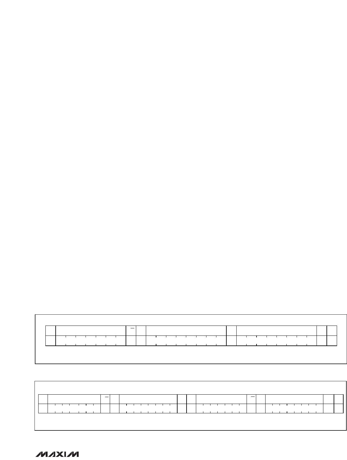
Register 0Bh Bit 0: Device Standby Command
When register 0Bh bit 0 is set to 1, the IC enters a low-
current standby mode. In this mode, the system clock is
off and no operation is allowed. Set this bit to 0 to leave
standby mode and back to normal operation mode.
Register 0Ch Bit 2-0: Device Revision Code
These 3 bits are a hardwired value that identifies the
IC’s revision.
Applications Information
Programming LED Currents
The MAX16826 uses sense resistors (R28, R29, R30,
R31 in the
Typical Application Circuit
) to set the output
current for each LED string. To set the LED current for a
particular string, connect a sense resistor across the
corresponding current-sense input (CS1–CS4) and
GND. For optimal accuracy, connect the low-side of the
current-sense resistors to GND with short traces. The
value needed for the sense resistor for a given current
is calculated with the equation below:
R31 = V
CS1
/I
OUT1
where V
CS1
can be set from 97mV to 316mV by the
internal registers through the I
2
C interface and I
OUT1
is
the desired LED string 1 current.
Calculating the Value of Peak
Current-Limit Resistor
The value of R12 sets the peak switching current that
flows in the switching FET (Q1). Set the value of resistor
R12 using the equation below:
R12 = 0.19/(1.2 x I
PK
)
where I
PK
is the peak inductor current at minimum input
voltage and maximum load.
Boost Inductor Value
The value of the boost inductor is calculated using the
following equation:
where V
INMIN
is the minimum input voltage, V
OUT
is the
desired output voltage, and f
SW
is the switching fre-
quency, and ΔI
L
is the peak-to-peak ripple in the boost
inductor. Higher inductor values lead to lower ripple but
at a higher cost and size. Choose an inductor value
that gives peak-to-peak ripple current in the order of
30% to 40% of the average current in the inductor at
low-line and full-rated load. This choice of inductor is a
compromise between cost, size, and performance for
the boost converter.
Setting Output Voltage
Set the switch regulator output voltage by connecting
FB to the center of a resistive voltage-divider between
the switching regulator output and GND. V
FB
is regulat-
ed to a voltage from 0.88V to 1.25V (typ) set by an
internal register through the I
2
C interface. Choose R13
and R14 in the
Typical Application Circuit
for a reason-
able bias current in the resistive divider and use the fol-
lowing formula to set the output voltage:
V
OUT
= (1 + R13/R14) x V
FB
where V
FB
is the regulated voltage set by the internal
register.
Adaptive Voltage Optimization
The availability of the digitized switching regulator output
voltage and current sink drain voltages and the ability to
change the switching regulator output voltage provide
the ability to do adaptive voltage optimization. A slow
digital control loop is established with an external μC
closing the loop. Firmware residing in the external μC is
tasked to read each one of the current sink FET drain
voltages and select the minimum value of the four LED
strings. The minimum value is subtracted from the scaled
output voltage reading, and then the switching regulator
output is forced to maintain the difference required to
provide current regulation in the current sink FETs.
L1
V VV
V f I
INMIN OUT INMIN
OSWL
=
×
()
××
UT
Δ
MAX16826
Programmable, Four-String HB LED Driver with
Output-Voltage Optimization and Fault Detection
______________________________________________________________________________________ 21

MAX16826ATJ+

Mfr. #:
Manufacturer:
Maxim Integrated
Description:
LED Lighting Drivers Prog 4-String HB
Lifecycle:
New from this manufacturer.
Delivery:
DHL FedEx Ups TNT EMS
Payment:
T/T Paypal Visa MoneyGram Western Union