Detailed Description
The MAX16826 HB LED driver integrates a switching
regulator controller, a 4-channel linear current sink dri-
ver, a 7-bit ADC, and an I
2
C interface. The IC is
designed to operate from a 4.75V to 24V input voltage
range and can withstand automotive load dump tran-
sients up to 40V.
The current-mode switching regulator controller is con-
figurable as a boost or SEPIC converter to regulate the
voltage to drive the four strings of HB LEDs. Its program-
mable switching frequency (100kHz to 1MHz) allows the
use of a small inductor and filter capacitors. The four
current sink regulators use independent external current-
sense resistors to provide constant currents for each
string of LEDs. Four DIM inputs allow a very wide range
of independent pulsed dimming to each LED string. An
internal 7-bit ADC measures the drain voltage of the
external driver transistors to enable output voltage opti-
mization and fault monitoring of the LEDs. The
MAX16826 is capable of driving four strings of LEDs.
The number of LEDs in each string is only limited by the
topology of choice, the rating of the external compo-
nents, and the resolution of the ADC and internal DAC.
Simplified Block Diagram
31
IN
5V
V
CC
V
CC
PGND
DL
CS
OVP
COMP
FB
RTCT
GND
OVT
CURRENT-
MODE
PWM
BLOCK
SYNC/EN
CSS
DR4
7-BIT ADC
AND
SHORTED
STRING
FAULT
DECTECTION
DR3
DR2
DR1
LINEAR
CURRENT-
SINK
DRIVERS
CS4
CS3
CS2
CS1
DL4
DL3
DL2
DL1
I
2
C
STATE
MACHINE
DOUBLE-
BUFFERED
REGISTER
AND DACS
DIM4
DIM3
OVT
OVT
DIM2
DIM1
SDA
SCL
26V
SHUNT
GND
OVT
REF
V
CC
GND
RSC
MAX16826
29
28
25
22
19
26
23
20
17
27
24
21
18
16
15
14
13
9
32
1
30
8
10
6
7
4
5
2
3
11
12
MAX16826
Programmable, Four-String HB LED Driver with
Output-Voltage Optimization and Fault Detection
10 ______________________________________________________________________________________
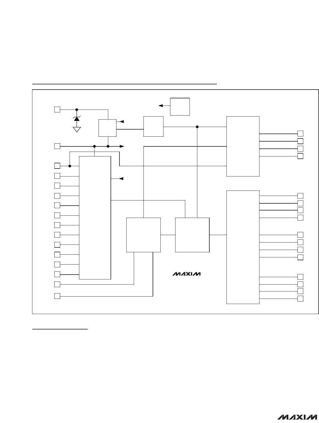
The MAX16826 provides additional flexibility with an
internal I
2
C serial interface to communicate with a
microcontroller (μC). The interface can be used to
dynamically adjust the amplitude of the LED current in
each LED string and the switch-mode regulator output
voltage. It can also be used to read the ADC drain volt-
age measurements for each string, allowing a μC to
dynamically adjust the output voltage to minimize the
power dissipation in the LED current sink FETs. The I
2
C
interface can also be used to detect faults such as LED
short or open.
Modes of Operation
The MAX16826 has six modes of operation: normal
mode, undervoltage lockout (UVLO) mode, thermal
shutdown (TSD) mode, shutdown (SHDN) mode,
standby (STBY) mode, and overvoltage protection
(OVP) mode.
The normal mode is the default state where each cur-
rent sink regulator is maintaining a constant current
through each of the LED strings. Digitized voltage feed-
back from the drains of the current sink FETs can be
used to establish a secondary control loop by using an
external μC to control the output of the switching stage
for the purpose of achieving low-power dissipation
across these FETs.
UVLO mode occurs when V
VCC
goes below 4.3V. In
UVLO mode, each of the linear current sinks and the
switching regulator is shut down until the input voltage
exceeds the rising UVLO threshold.
TSD mode occurs when the die temperature exceeds
the internally set thermal limit (+160°C). In TSD mode,
each of the linear regulators and the switching regulator
is shut down until the die temperature cools by 20°C.
SHDN mode occurs when SYNC/EN is driven low. In
SHDN mode, all internal circuitry with the exception of
the shunt regulator is deactivated to limit current draw
to less than 50μA. SHDN mode disengages when
SYNC/EN is driven high or clocked.
STBY mode is initiated using the I
2
C interface. In STBY
mode, each of the linear current sinks and the switching
regulator is shut down. STBY mode is also deactivated
using the I
2
C interface. In STBY mode, the internal V
CC
regulator and the shunt regulator remain active. Whenever
the MAX16826 enters a mode that deactivates the switch-
ing regulator, the soft-start capacitor is discharged so that
soft-start occurs upon reactivation.
OVP mode occurs when the voltage at OVP is higher than
the internal reference. In OVP mode, the switching regula-
tor gate-drive output is latched off and can only be
restored by cycling enable, power, or entering standby
mode.
Switching Preregulator Stage
The MAX16826 features a current-mode controller that
is capable of operating in the frequency range of
100kHz to 1MHz. Current-mode control provides fast
response and simplifies loop compensation.
Output voltage regulation can be achieved in a two-
loop configuration. A required conventional control loop
can be set up by using the internal error amplifier with
its inverting input connected to FB. The bandwidth of
this loop is set to be as high as possible utilizing con-
ventional compensation techniques. The noninverting
input of this amplifier is connected to a reference volt-
age that is dynamically adjustable using the I
2
C inter-
face. The optional slower secondary loop consists of
the external μC using the I
2
C interface reading out the
voltages at the drains of the current sink FETs and
adjusting the reference voltage for the error amplifier.
To regulate the output voltage, the error amplifier com-
pares the voltage at FB to the internal 1.25V (adjustable
down by using the I
2
C interface) reference. The output
of the error amplifier is compared to the sum of the cur-
rent-sense signal and the slope compensation ramp at
RSC to control the duty cycle at DL.
Two current-limit comparators also monitor the voltage
across the sense resistor using CS. If the primary cur-
rent-limit threshold is reached, the FET is turned off and
remains off for the reminder of the switching cycle. If
the current through the FET reaches the secondary cur-
rent limit, the switching cycle is terminated and the soft-
start capacitor is discharged. The converter then
restarts in soft-start mode preventing inductor current
runaway due to the delay of the primary cycle-by-cycle
current limit. The switching regulator controller also fea-
tures an overvoltage protection circuit that latches the
gate driver off if the voltage at OVP exceeds the inter-
nal 1.25V reference voltage.
MAX16826
Programmable, Four-String HB LED Driver with
Output-Voltage Optimization and Fault Detection
______________________________________________________________________________________ 11
MAX16826
Shunt Regulator
The MAX16826 has an internal 26V (typ) shunt regula-
tor to provide the primary protection against an auto-
motive load dump. When the input voltage is below
26V, the shunt voltage at IN tracks the input voltage.
When the input voltage exceeds 26V, the shunt regula-
tor turns on to sink current, and the voltage at IN is
clamped to 26V. During a load dump, the input voltage
can reach 40V, and the shunt regulator through the
resistor connected to IN is forced to sink large amounts
of current for up to 400ms to limit the voltage that
appears at IN to the shunt regulation voltage. The sink-
ing current of the shunt regulator is limited by the value
of resistor (R1 in Figure 1) in series with IN. There are
two criteria that determine the value of R1: the maxi-
mum acceptable shunt current during load dump, and
the voltage drop on R1 under normal operating condi-
tions with low battery voltage. For example, with typical
20mA input current in normal operation, 250mA load
dump current limit, 40V maximum load dump voltage,
the R1 value is:
where V
INMIN
is the minimum operating voltage and
V
INREG
is the minimum acceptable voltage at IN.
Use the following equation to verify that the current
through R1 is less than 250mA under a load-dump con-
dition:
For stable operation, the shunt regulator requires a min-
imum 10μF of ceramic capacitance from IN to GND.
V
CC
Regulator
The 5.25V V
CC
regulator provides bias for the internal
circuitry including the bandgap reference and gate dri-
vers. Externally bypass V
CC
with a minimum 4.7μF
ceramic capacitor. V
CC
has the ability to supply up to
50mA of current, but external loads should be mini-
mized so as not to take away drive capability for inter-
nal circuitry. If IN is powered by a voltage less than
5.5V, connect V
CC
directly to IN.
Switch-Mode Controller
The MAX16826 consists of a current-mode controller
that is capable of operating in the 100kHz to 1MHz fre-
quency range (Figure 2). Current-mode control pro-
vides fast response and simplifies loop compensation.
The error amplifier compares the voltage at FB to 1.25V
and varies the COMP output accordingly to regulate.
The PWM comparator compares the voltage at COMP
with the voltage at RSC to determine the switching duty
cycle. The primary cycle-by-cycle current-limit com-
parator interrupts the on-time if the sense voltage is
larger than 200mV. When the sense voltage is larger
than 270mV, the secondary gross current-limit com-
parator is activated to discharge the soft-start capaci-
tor. This forces the IC to re-soft-start preventing
inductor current runaway due to the delay of the prima-
ry cycle-by-cycle current limit.
The switch-mode controller also features a low current
shutdown mode, adjustable soft-start, and thermal
shutdown protection.
I
VV
R
mA
LD
LD
===
−−26
1
40 26
100
140
R
VV
I
INMIN INREG
Q
1
75 55
20 10
100
3
==
×
=
−−
..
Ω
Programmable, Four-String HB LED Driver with
Output-Voltage Optimization and Fault Detection
12 ______________________________________________________________________________________
MAX16826
5V
REFERENCE
+
-
R1
IN
V
IN
C4
Figure 1. Shunt Regulator Block Diagram

MAX16826ATJ+

Mfr. #:
Manufacturer:
Maxim Integrated
Description:
LED Lighting Drivers Prog 4-String HB
Lifecycle:
New from this manufacturer.
Delivery:
DHL FedEx Ups TNT EMS
Payment:
T/T Paypal Visa MoneyGram Western Union