MAX16826
is 2μs, so the ADC requires at least 5 of these minimum
pulses within the 190ms measurement window to com-
plete a conversion. During PWM dimming, LED current
pulse widths of less than 2μs are possible, but the ADC
may not have enough sampling time to complete a con-
version in this scenario and the corresponding data may
be incomplete or inaccurate. Therefore, adaptive volt-
age optimization may not be possible when the LED
current-pulse duration is less than 2μs. The LED current
pulse duration is shorter than the pulse applied at the
DIM_ inputs because of the LED turn-on delay.
Faults and Fault Detection
The MAX16826 features circuitry that automatically
detects faults such as overvoltage or shorted LED string.
An internal fault register at the address OAh is used to
record these faults. For example, if a shorted LED string
is detected, the corresponding fault register bit is set and
the faulty output is shut down.
Shorted LED strings are detected with fast comparators
connected to DR1–DR4. The trip threshold of these
comparators is 1.52V (typ). When this threshold is
exceeded, the shorted string is latched off and the cor-
responding bit of register OAh is set.
After the internal ADC completes a conversion, the
result is stored in the corresponding register and can
be read out by the external μC. The μC then compares
the conversion data with the preset limit to determine if
there is a fault.
When an LED string opens, the voltage at the corre-
sponding current-sink FET drain node goes to 0V.
However, the ADC can only complete a conversion if
the LED current comes into regulation. If an LED string
opens before the LED current can come into regulation,
the ADC cannot complete a conversion and the MSB
(eighth bit) is set to indicate an incomplete conversion
or timeout condition. Thus, an examination of the MSB
provides an indication that the LED string is open. If the
LED string opens after the LED current is in regulation,
the ADC can make conversions and reports that the
drain voltage is 0V. Therefore, to detect an open condi-
tion, monitor the MSB and the ADC measurement. If the
MSB is set and the CS_ on-time is greater than 2μs, or
if the ADC measures 0 at the drain, then there is an
open circuit.
Programmable, Four-String HB LED Driver with
Output-Voltage Optimization and Fault Detection
16 ______________________________________________________________________________________
Table 1. ADC Response
CONDITION ADC RESPONSE
Shorted string fault
Load full-scale code into register, no conversions on affected channel until power or enable is
cycled.
Shorted string fault while
converting
Immediately load full-scale code into register and cease conversion effort on this channel until
power or enable is cycled.
ADC register read when it is
being updated
Previous sample is shifted out through the I
2
C interface and then the register is updated with the
new measurement.
UVLO Immediately terminate conversions, do not update current register.
STBY Immediately terminate conversions, do not update current register.
SHDN Immediately terminate conversions, do not update current register.
REGISTER
FILE UNIT
ADC DAC
POWER
MANAGEMENT
OVP
I
2
C
SYSTEM
CLOCK
EXTERNAL
EVENTS
Figure 3. Digital Block Diagram
Overview of the Digital Section
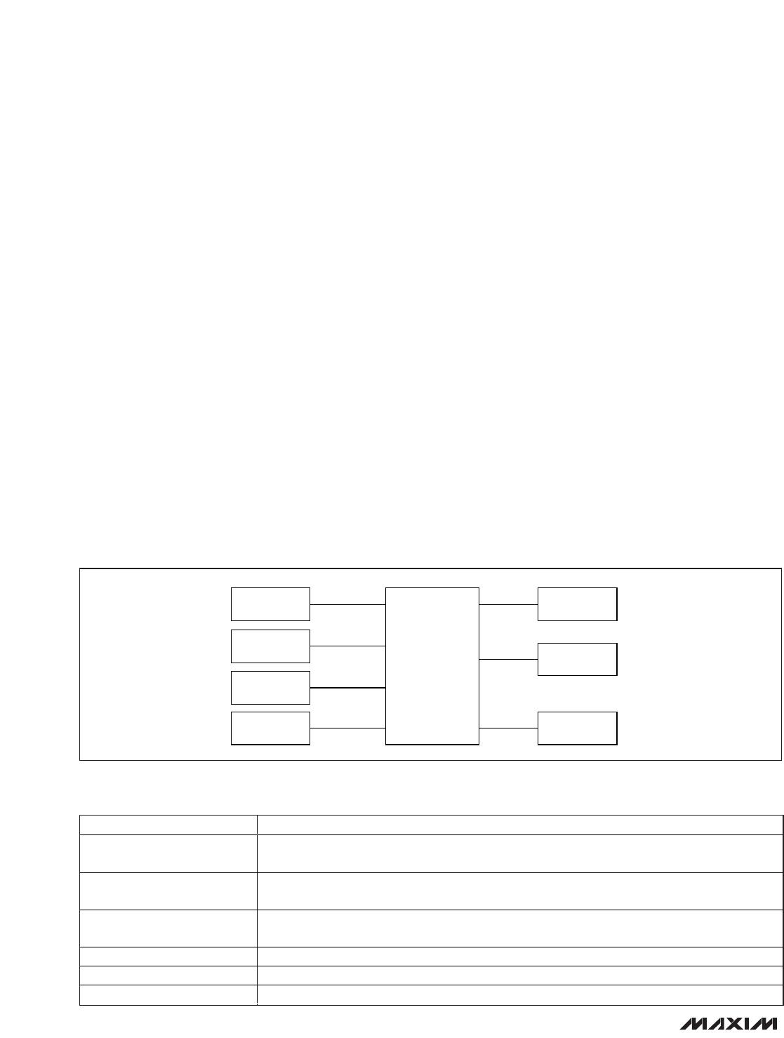
Figure 3 shows the block diagram of the digital section in
the MAX16826. The I
2
C serial interface provides flexible
control of the IC and is in charge of writing/reading
to/from the register file unit. The ADC block is a 7-bit
5-channel SAR ADC. The eighth bit of the ADC data reg-
ister indicates an incomplete conversion or timeout has
occurred. This bit is set whenever the LED current fails to
come into regulation during the DIM PWM on-time. This
indicates there is either an LED open condition or the
CS_ on-time is less than 2μs.
A reason for this among other possibilities is an open
LED string condition. This eighth or MSB bit can be
tested to determine open string faults.
I
2
C Interface
The MAX16826 internal I
2
C serial interface provides
flexible control of the amplitude of the LED current in
each string and the switch-mode regulator output volt-
age. It is also able to read the current sink FET drain
voltages, as well as the switching regulator output volt-
age through OVP and thus enable some fault detection
and power dissipation minimization. By using an exter-
nal μC, the MAX16826 internal control and status regis-
ters are also accessed through the standard
bidirectional, 2-wire, I
2
C serial interface.
The I
2
C interface provides the following I/O functions
and programmability:
Current sink FET drain and switching regulator out-
put-voltage measurement. The measurement for
each channel and the regulator output is stored in
its respective register and can be accessed
through the I
2
C interface. The SAR ADC measures
the drain voltage of each current sink FET sequen-
tially. This uses one 8-bit register for each channel
to store the measurement made by the 7-bit SAR
ADC and 1 bit to indicate a timeout during the ADC
conversion cycle.
Adjustment of the switching regulator output. This is
used for adaptive voltage optimization to improve
overall efficiency. The switching regulator output is
downward adjustable by changing its reference
voltage. This uses a 7-bit register.
Adjustment of the reference voltage of the current-
sink regulators. The reference voltage at the nonin-
verting input of each of the linear regulator drive
amplifiers can be changed to make adjustments in
the current of each LED string for a given sense
resistor. The output can be adjusted down from a
maximum of 316mV to 97mV in 1.72mV increments.
Fault reporting. When a shorted string fault or an
overvoltage fault occurs, the fault is recorded.
Standby mode. When a one is entered into the
standby register the IC goes into standby mode.
The 7-bit I
2
C address is 58h and the 8-bit I
2
C address
is B1h for a read operation and B0h for a write opera-
tion. Address the MAX16826 using the I
2
C interface to
read the state of the registers or to write to the registers.
Upon a read command, the MAX16826 transmits the
data in the register that the address register is pointing
to. This is done so that the user has the ability to confirm
the data written to a register before the output is
enabled. Use the fault register to diagnose any faults.
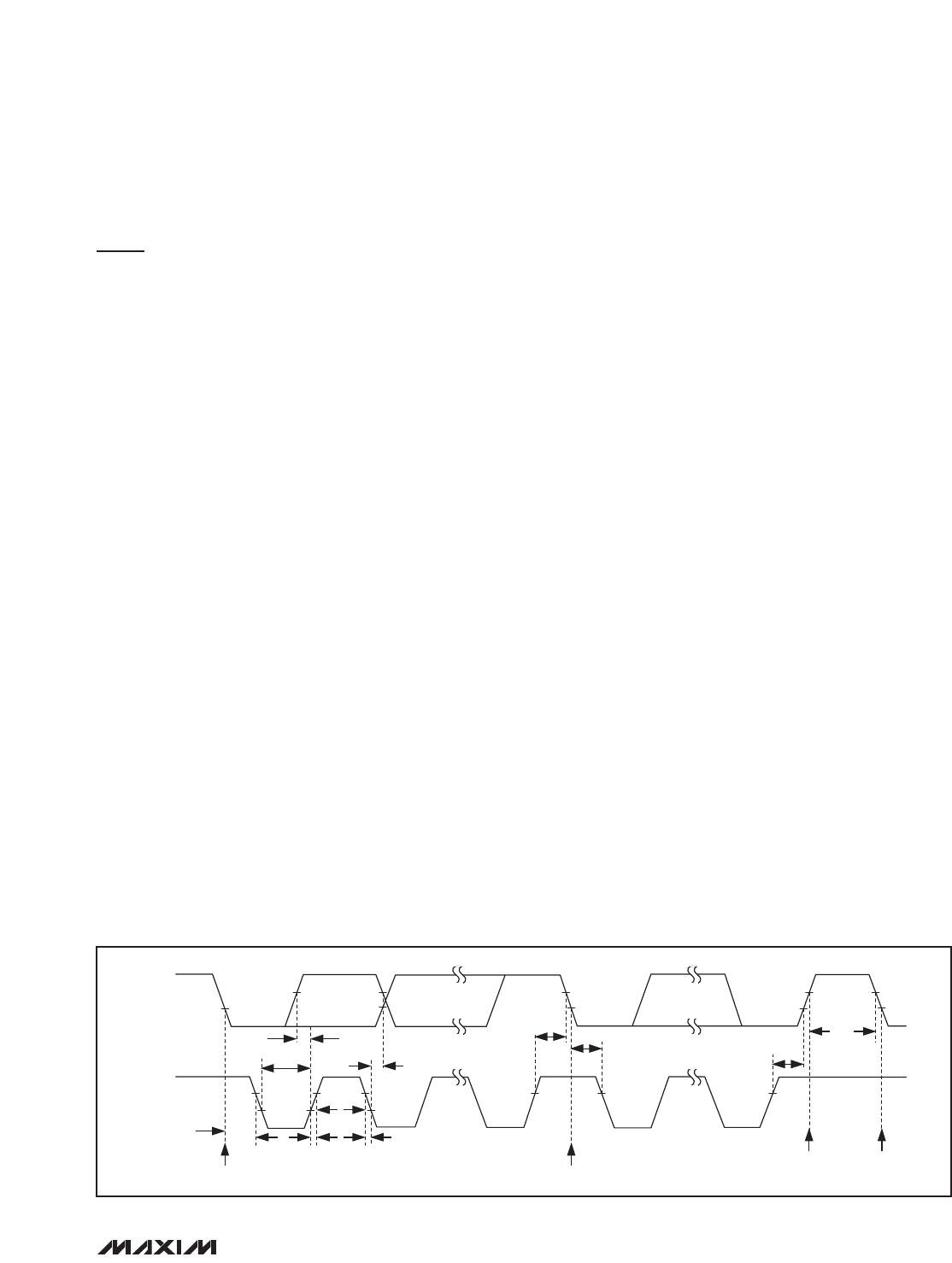
Serial Addressing
The I
2
C interface consists of a serial data line (SDA)
and a serial clock line (SCL) to achieve bidirectional
communication between the master and the slave. The
MAX16826 is a slave-only device, relying upon a mas-
ter to generate a clock signal. The master initiates data
transfer to and from the MAX16826 and generates SCL
to synchronize the data transfer (Figure 4).
MAX16826
Programmable, Four-String HB LED Driver with
Output-Voltage Optimization and Fault Detection
______________________________________________________________________________________ 17
SCL
SDA
t
R
t
F
t
BUF
START
CONDITION
STOP
CONDITION
REPEATED START CONDITION
START CONDITION
t
SU,STO
t
HD,STA
t
SU,STA
t
HD,DAT
t
SU,DAT
t
LOW
t
HIGH
t
HD,STA
Figure 4. 2-Wire Serial Interface Timing Detail
MAX16826
I
2
C is an open-drain bus. Both SDA and SCL are bidi-
rectional lines, connected to a positive supply voltage
using a pullup resistor. They both have Schmitt triggers
and filter circuits to suppress noise spikes on the bus to
ensure proper device operation.
A bus master initiates communication with the
MAX16826 as a slave device by issuing a START con-
dition followed by the MAX16826 address. The
MAX16826 address byte consists of 7 address bits and
a read/write bit (R/W). After receiving the proper
address, the MAX16826 issues an acknowledge bit by
pulling SDA low during the ninth clock cycle.
START and STOP Conditions
Both SCL and SDA remain high when the bus is not
busy. The master signals the beginning of a transmis-
sion with a START (S) condition by transitioning SDA
from high to low while SCL is high. When the master
has finished communicating with the MAX16826, it
issues a STOP (P) condition by transitioning SDA from
low to high while SCL is high. The bus is then free for
another transmission (Figure 4). Both START and STOP
conditions are generated by the bus master.
Bit Transfer
Each data bit, from the most significant bit to the least
significant bit, is transferred one by one during each
clock cycle. During data transfer, the SDA signal is
allowed to change only during the low period of the
SCL clock and it must remain stable during the high
period of the SCL clock (Figure 5).
Acknowledge
The acknowledge bit is used by the recipient to hand-
shake the receipt of each byte of data (Figure 6). After
data transfer, the master generates the acknowledge
clock pulse and the recipient pulls down the SDA line
during this acknowledge clock pulse, such that the
SDA line stays low during the high duration of the clock
pulse. When the master transmits the data to the
MAX16826, it releases the SDA line and the MAX16826
takes the control of SDA line and generates the
acknowledge bit. When SDA remains high during this
9th clock pulse, this is defined as the not acknowledge
signal. The master then generates either a STOP condi-
tion to abort the transfer, or a repeated START condi-
tion to start a new transfer.
Programmable, Four-String HB LED Driver with
Output-Voltage Optimization and Fault Detection
18 ______________________________________________________________________________________
START
CONDITION
(S)
DATA LINE STABLE
DATA VALID
DATA ALLOWED
TO CHANGE
STOP
CONDITION
(P)
SCL
SDA
Figure 5. Bit Transfer
SCL
SDA
BY MASTER
1
289
S
START CONDITION CLOCK PULSE FOR ACKNOWLEDGMENT
SDA
BY SLAVE
Figure 6. Acknowledge

MAX16826ATJ+

Mfr. #:
Manufacturer:
Maxim Integrated
Description:
LED Lighting Drivers Prog 4-String HB
Lifecycle:
New from this manufacturer.
Delivery:
DHL FedEx Ups TNT EMS
Payment:
T/T Paypal Visa MoneyGram Western Union