xxxxxxxxxxxxxxxxxxxxx xxxxxxxxxxxxxxxxxxxxxxxxxx xxxxxxx x x x xxxxxxxxxxxxxxxxxxxxxxxxxxxxxx xxxxxxxxxxxxxxxxxxx xx xx xxxxx
xxxxxxxxxxxxxxxxxxxxxxxxxxx xxxxxxxxxxxxxxxxxxx xxxxxx xxxxxxxxxxxxxxxxxxxxxxxxxxxxxxxxxxx xxxxxxxxxxxx x x
xxxxxxxxxxxxxxxxxxxxx xxxxxxxxxxxxxxxxxxxxxxxxxxxxxx xxxxx xxxxxxxxxxxxxxxxxxxxxxxxxxxxxxxxxxxxxxxxxxxxxxxxxx xxxxxxxx
xxxxxxxxxxxxxxxxxxxxxxxxx xxxxxxxxxxxxxxxxxxxx xxx
PCA9555 All information provided in this document is subject to legal disclaimers. © NXP Semiconductors N.V. 2017. All rights reserved.
Product data sheet Rev. 10 — 8 November 2017 10 of 34
NXP Semiconductors
PCA9555
16-bit I
2
C-bus and SMBus I/O port with interrupt
Fig 9. Write to Output port registers
1 0 0 A2 A1 A0 0 AS0
START condition R/W acknowledge
from slave
002aac220
A
SCL
SDA A
write to port
data out
from port 0
P
t
v(Q)
987654321
command byte
data to port 0
DATA 0
slave address
00000100
STOP
condition
0.00.7
acknowledge
from slave
acknowledge
from slave
data to port 1
DATA 1 1.01.7
A
data out
from port 1
t
v(Q)
DATA VALID
Fig 10. Write to Configuration registers
1 0 0 A2 A1 A0 0 AS0
START condition R/W acknowledge
from slave
002aac221
A
SCL
SDA A P
987654321
command byte
data to register
DATA 0
slave address
00001100
STOP
condition
LSBMSB
acknowledge
from slave
acknowledge
from slave
data to register
DATA 1
LSBMSB
A
PCA9555 All information provided in this document is subject to legal disclaimers. © NXP Semiconductors N.V. 2017. All rights reserved.
Product data sheet Rev. 10 — 8 November 2017 11 of 34
NXP Semiconductors
PCA9555
16-bit I
2
C-bus and SMBus I/O port with interrupt
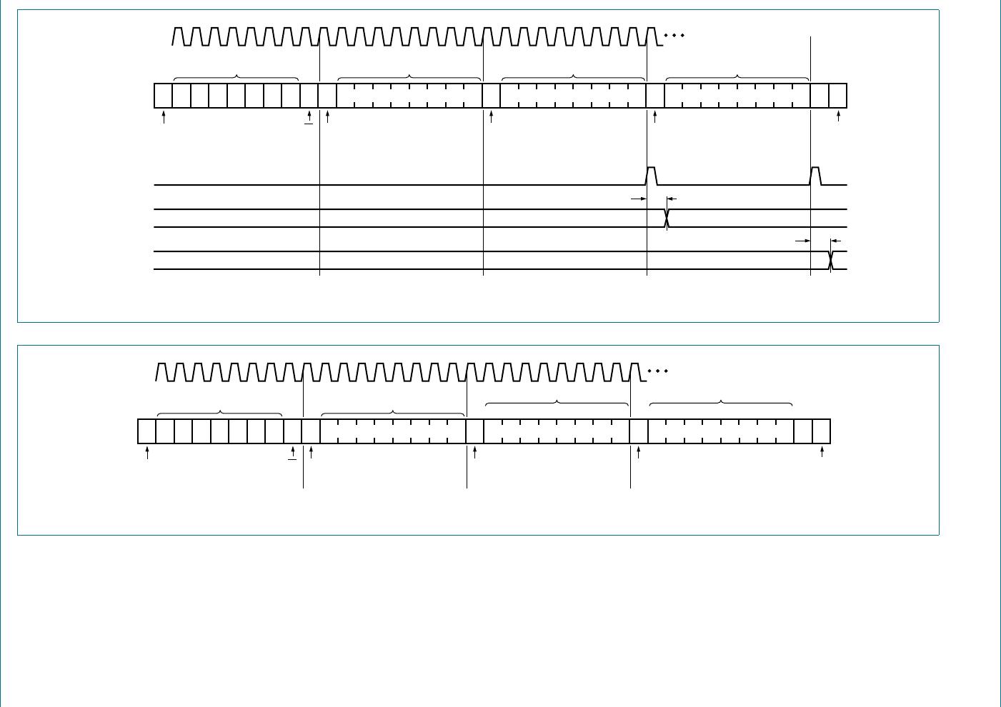
6.5.2 Reading the port registers
In order to read data from the PCA9555, the bus master must first send the PCA9555
address with the least significant bit set to a logic 0 (see Figure 7 “
PCA9555 device
address). The command byte is sent after the address and determines which register will
be accessed. After a restart, the device address is sent again, but this time the least
significant bit is set to a logic 1. Data from the register defined by the command byte will
then be sent by the PCA9555 (see Figure 11
, Figure 12 and Figure 13). Data is clocked
into the register on the falling edge of the acknowledge clock pulse. After the first byte is
read, additional bytes may be read but the data will now reflect the information in the other
register in the pair. For example, if you read Input Port 1, then the next byte read would be
Input Port 0. There is no limitation on the number of data bytes received in one read
transmission but the final byte received, the bus master must not acknowledge the data.
Remark: Transfer can be stopped at any time by a STOP condition.
Fig 11. Read from register
AS
START condition R/W
acknowledge
from slave
002aac222
A
acknowledge
from slave
SDA
A P
acknowledge
from master
DATA (first byte)
slave address
STOP
condition
S
(repeated)
START condition
(cont.)
(cont.)
1 0 0 A2 A1 A0 1 A0
R/W
acknowledge
from slave
slave address
at this moment master-transmitter becomes master-receiver
and slave-receiver becomes slave-transmitter
NA
no acknowledge
from master
COMMAND BYTE
1 0 0 A2 A1 A00 0
data from lower or
upper byte of register
LSBMSB
DATA (last byte)
data from upper or
lower byte of register
LSBMSB
xxxxxxxxxxxxxxxxxxxxx xxxxxxxxxxxxxxxxxxxxxxxxxx xxxxxxx x x x xxxxxxxxxxxxxxxxxxxxxxxxxxxxxx xxxxxxxxxxxxxxxxxxx xx xx xxxxx
xxxxxxxxxxxxxxxxxxxxxxxxxxx xxxxxxxxxxxxxxxxxxx xxxxxx xxxxxxxxxxxxxxxxxxxxxxxxxxxxxxxxxxx xxxxxxxxxxxx x x
xxxxxxxxxxxxxxxxxxxxx xxxxxxxxxxxxxxxxxxxxxxxxxxxxxx xxxxx xxxxxxxxxxxxxxxxxxxxxxxxxxxxxxxxxxxxxxxxxxxxxxxxxx xxxxxxxx
xxxxxxxxxxxxxxxxxxxxxxxxx xxxxxxxxxxxxxxxxxxxx xxx
PCA9555 All information provided in this document is subject to legal disclaimers. © NXP Semiconductors N.V. 2017. All rights reserved.
Product data sheet Rev. 10 — 8 November 2017 12 of 34
NXP Semiconductors
PCA9555
16-bit I
2
C-bus and SMBus I/O port with interrupt
Remark: Transfer of data can be stopped at any moment by a STOP condition. When this occurs, data present at the latest acknowledge phase is valid (output mode). It
is assumed that the command byte has previously been set to ‘00’ (read Input Port register).
Fig 12. Read Input port register, scenario 1
1 0 0 A2 A1 A0 1 AS0
START condition
R/W
acknowledge
from slave
002aac223
A
SCL
SDA A
read from port 0
P
987654321
I0.xslave address
STOP condition
acknowledge
from master
A
I1.x
acknowledge
from master
A
I0.x
acknowledge
from master
1
I1.x
non acknowledge
from master
data into port 0
read from port 1
data into port 1
INT
65432107 65432107 65432107 65432107
INT
t
v(INT_N)
t
rst(INT_N)

PCA9555PW,118

Mfr. #:
Manufacturer:
NXP Semiconductors
Description:
Interface - I/O Expanders 16-BIT I2C FM TP GPIO INT PU
Lifecycle:
New from this manufacturer.
Delivery:
DHL FedEx Ups TNT EMS
Payment:
T/T Paypal Visa MoneyGram Western Union