xxxxxxxxxxxxxxxxxxxxx xxxxxxxxxxxxxxxxxxxxxxxxxx xxxxxxx x x x xxxxxxxxxxxxxxxxxxxxxxxxxxxxxx xxxxxxxxxxxxxxxxxxx xx xx xxxxx
xxxxxxxxxxxxxxxxxxxxxxxxxxx xxxxxxxxxxxxxxxxxxx xxxxxx xxxxxxxxxxxxxxxxxxxxxxxxxxxxxxxxxxx xxxxxxxxxxxx x x
xxxxxxxxxxxxxxxxxxxxx xxxxxxxxxxxxxxxxxxxxxxxxxxxxxx xxxxx xxxxxxxxxxxxxxxxxxxxxxxxxxxxxxxxxxxxxxxxxxxxxxxxxx xxxxxxxx
xxxxxxxxxxxxxxxxxxxxxxxxx xxxxxxxxxxxxxxxxxxxx xxx
PCA9555 All information provided in this document is subject to legal disclaimers. © NXP Semiconductors N.V. 2017. All rights reserved.
Product data sheet Rev. 10 — 8 November 2017 13 of 34
NXP Semiconductors
PCA9555
16-bit I
2
C-bus and SMBus I/O port with interrupt
Remark: Transfer of data can be stopped at any moment by a STOP condition. When this occurs, data present at the latest acknowledge phase is valid (output mode). It
is assumed that the command byte has previously been set to ‘00’ (read Input Port register).
Fig 13. Read Input port register, scenario 2
1 0 0 A2 A1 A0 1 AS0
START condition
R/W
acknowledge
from slave
002aac224
A
SCL
SDA A
read from port 0
P
987654321
I0.xslave address
STOP condition
acknowledge
from master
A
I1.x
acknowledge
from master
A
I0.x
acknowledge
from master
1
I1.x
non acknowledge
from master
data into port 0
read from port 1
data into port 1
INT
t
v(INT_N)
t
rst(INT_N)
DATA 00 DATA 10 DATA 03 DATA 12
DATA 00 DATA 01
t
h(D)
t
h(D)
DATA 02
t
su(D)
DATA 03
t
su(D)
DATA 10 DATA 11 DATA 12
PCA9555 All information provided in this document is subject to legal disclaimers. © NXP Semiconductors N.V. 2017. All rights reserved.
Product data sheet Rev. 10 — 8 November 2017 14 of 34
NXP Semiconductors
PCA9555
16-bit I
2
C-bus and SMBus I/O port with interrupt
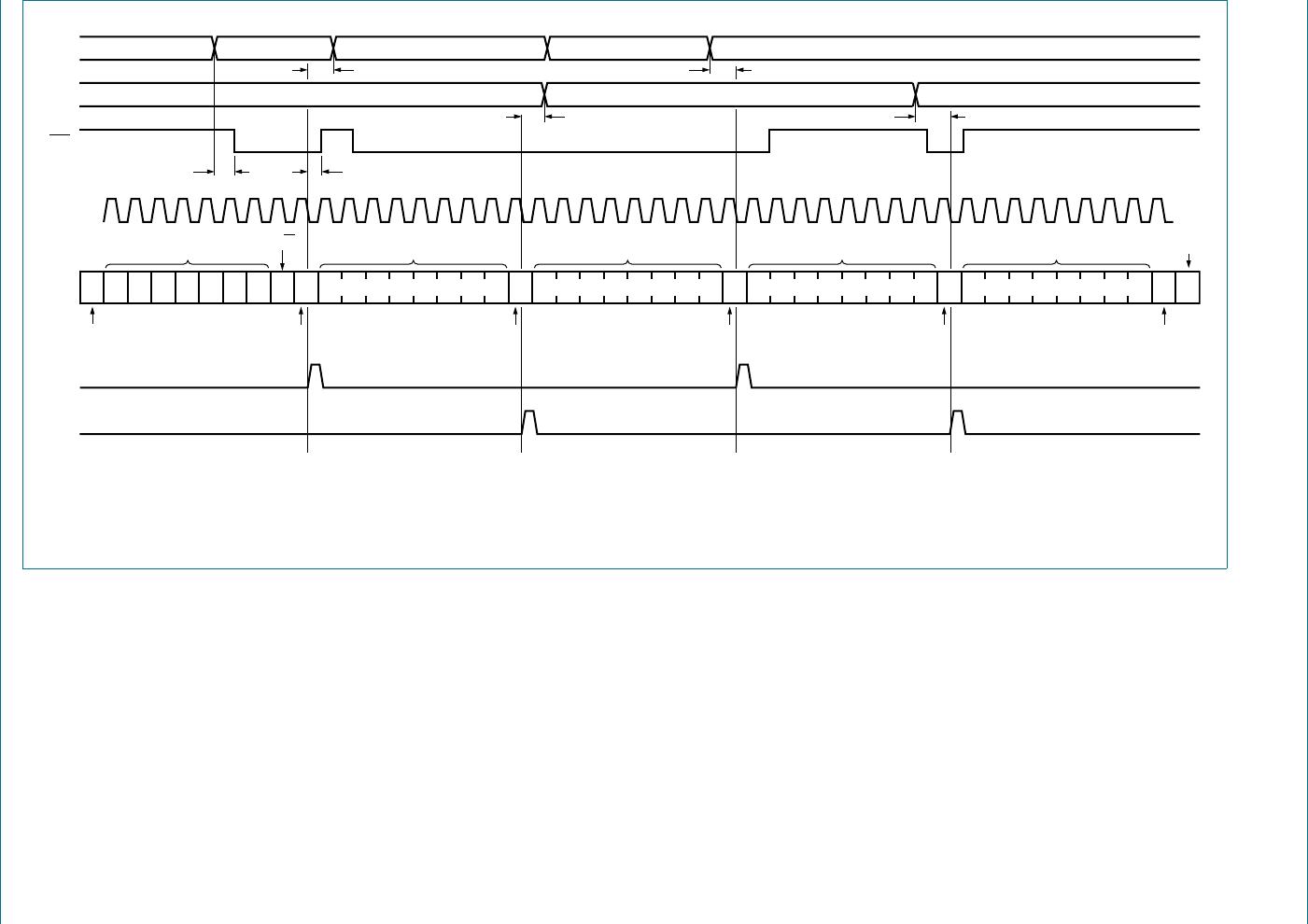
6.5.3 Interrupt output
The open-drain interrupt output is activated when one of the port pins changes state and
the pin is configured as an input. The interrupt is deactivated when the input returns to its
previous state or the Input Port register is read (see Figure 12
). A pin configured as an
output cannot cause an interrupt. Since each 8-bit port is read independently, the interrupt
caused by Port 0 will not be cleared by a read of Port 1 or the other way around.
Remark: Changing an I/O from an output to an input may cause a false interrupt to occur
if the state of the pin does not match the contents of the Input Port register.
7. Characteristics of the I
2
C-bus
The I
2
C-bus is for 2-way, 2-line communication between different ICs or modules. The two
lines are a serial data line (SDA) and a serial clock line (SCL). Both lines must be
connected to a positive supply via a pull-up resistor when connected to the output stages
of a device. Data transfer may be initiated only when the bus is not busy.
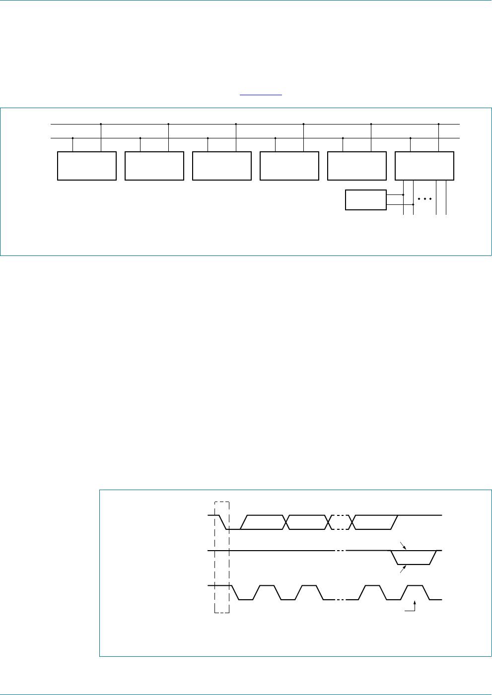
7.1 Bit transfer
One data bit is transferred during each clock pulse. The data on the SDA line must remain
stable during the HIGH period of the clock pulse as changes in the data line at this time
will be interpreted as control signals (see Figure 14
).
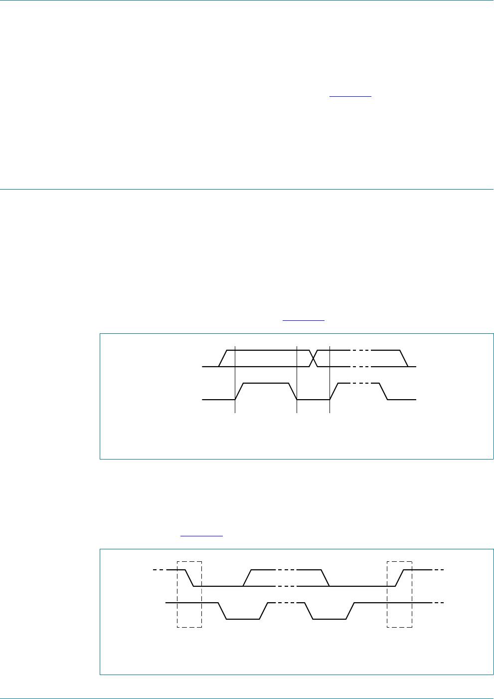
7.1.1 START and STOP conditions
Both data and clock lines remain HIGH when the bus is not busy. A HIGH-to-LOW
transition of the data line while the clock is HIGH is defined as the START condition (S). A
LOW-to-HIGH transition of the data line while the clock is HIGH is defined as the STOP
condition (P) (see Figure 15
).
Fig 14. Bit transfer
mba607
data line
stable;
data valid
change
of data
allowed
SDA
SCL
Fig 15. Definition of START and STOP conditions
mba608
SDA
SCL
P
STOP condition
S
START condition
PCA9555 All information provided in this document is subject to legal disclaimers. © NXP Semiconductors N.V. 2017. All rights reserved.
Product data sheet Rev. 10 — 8 November 2017 15 of 34
NXP Semiconductors
PCA9555
16-bit I
2
C-bus and SMBus I/O port with interrupt
7.2 System configuration
A device generating a message is a ‘transmitter’; a device receiving is the ‘receiver’. The
device that controls the message is the ‘master’ and the devices which are controlled by
the master are the ‘slaves’ (see Figure 16
).
7.3 Acknowledge
The number of data bytes transferred between the START and the STOP conditions from
transmitter to receiver is not limited. Each byte of eight bits is followed by one
acknowledge bit. The acknowledge bit is a HIGH level put on the bus by the transmitter,
whereas the master generates an extra acknowledge related clock pulse.
A slave receiver which is addressed must generate an acknowledge after the reception of
each byte. Also a master must generate an acknowledge after the reception of each byte
that has been clocked out of the slave transmitter. The device that acknowledges has to
pull down the SDA line during the acknowledge clock pulse, so that the SDA line is stable
LOW during the HIGH period of the acknowledge related clock pulse; set-up time and hold
time must be taken into account.
A master receiver must signal an end of data to the transmitter by not generating an
acknowledge on the last byte that has been clocked out of the slave. In this event, the
transmitter must leave the data line HIGH to enable the master to generate a STOP
condition.
Fig 16. System configuration
002aaa966
MASTER
TRANSMITTER/
RECEIVER
SLAVE
RECEIVER
SLAVE
TRANSMITTER/
RECEIVER
MASTER
TRANSMITTER
MASTER
TRANSMITTER/
RECEIVER
SDA
SCL
I
2
C-BUS
MULTIPLEXER
SLAVE
Fig 17. Acknowledgement on the I
2
C-bus
002aaa987
S
START
condition
9821
clock pulse for
acknowledgement
not acknowledge
acknowledge
data output
by transmitter
data output
by receiver
SCL from master

PCA9555PW,118

Mfr. #:
Manufacturer:
NXP Semiconductors
Description:
Interface - I/O Expanders 16-BIT I2C FM TP GPIO INT PU
Lifecycle:
New from this manufacturer.
Delivery:
DHL FedEx Ups TNT EMS
Payment:
T/T Paypal Visa MoneyGram Western Union