PCA9555 All information provided in this document is subject to legal disclaimers. © NXP Semiconductors N.V. 2017. All rights reserved.
Product data sheet Rev. 10 — 8 November 2017 28 of 34
NXP Semiconductors
PCA9555
16-bit I
2
C-bus and SMBus I/O port with interrupt
Process issues, such as application of adhesive and flux, clinching of leads, board
transport, the solder wave parameters, and the time during which components are
exposed to the wave
Solder bath specifications, including temperature and impurities
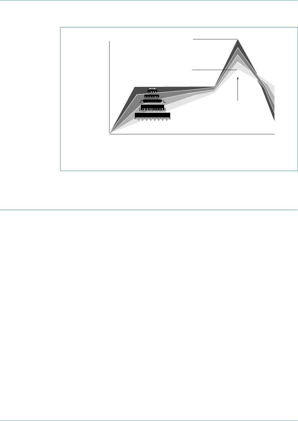
15.4 Reflow soldering
Key characteristics in reflow soldering are:
Lead-free versus SnPb soldering; note that a lead-free reflow process usually leads to
higher minimum peak temperatures (see Figure 30
) than a SnPb process, thus
reducing the process window
Solder paste printing issues including smearing, release, and adjusting the process
window for a mix of large and small components on one board
Reflow temperature profile; this profile includes preheat, reflow (in which the board is
heated to the peak temperature) and cooling down. It is imperative that the peak
temperature is high enough for the solder to make reliable solder joints (a solder paste
characteristic). In addition, the peak temperature must be low enough that the
packages and/or boards are not damaged. The peak temperature of the package
depends on package thickness and volume and is classified in accordance with
Table 16
and 17
Moisture sensitivity precautions, as indicated on the packing, must be respected at all
times.
Studies have shown that small packages reach higher temperatures during reflow
soldering, see Figure 30
.
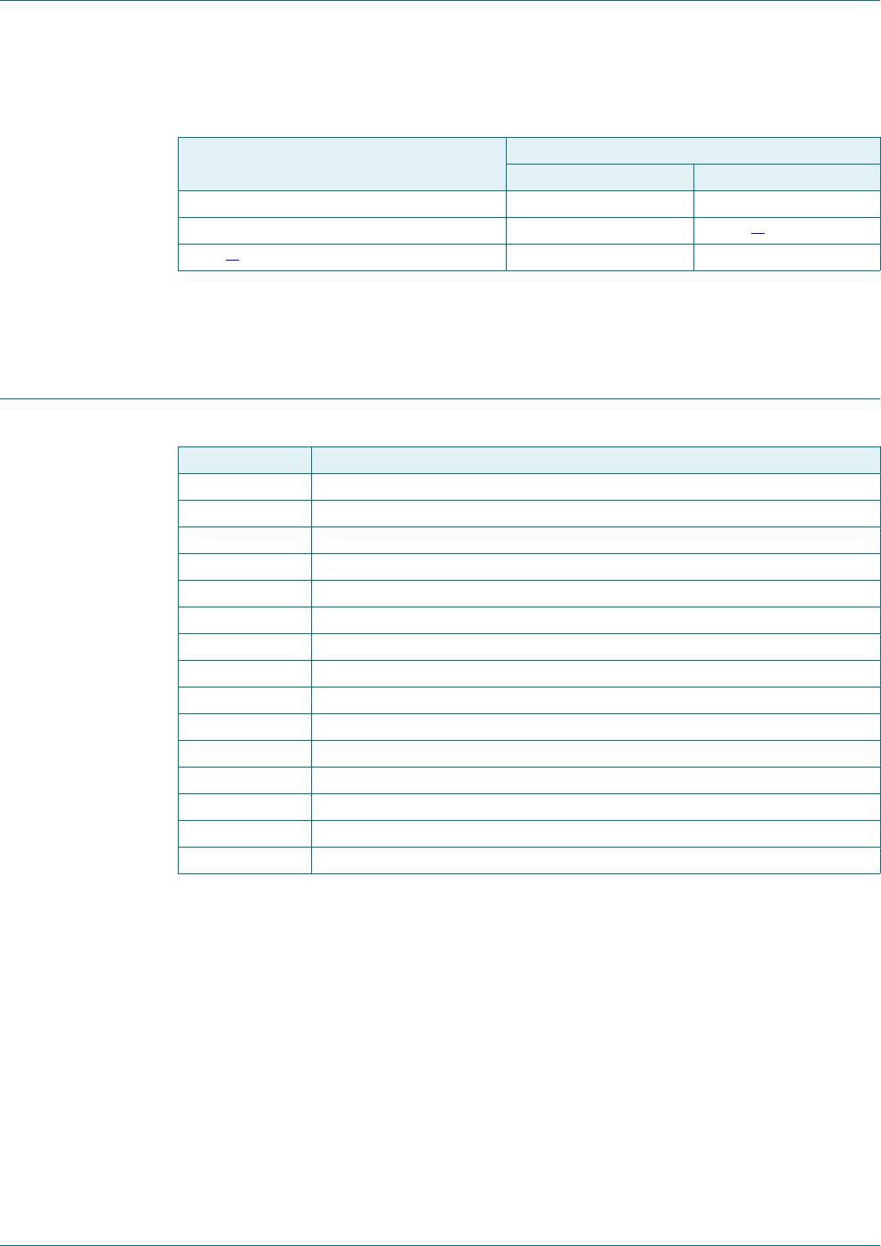
Table 16. SnPb eutectic process (from J-STD-020C)
Package thickness (mm) Package reflow temperature (C)
Volume (mm
3
)
< 350 350
< 2.5 235 220
2.5 220 220
Table 17. Lead-free process (from J-STD-020C)
Package thickness (mm) Package reflow temperature (C)
Volume (mm
3
)
< 350 350 to 2000 > 2000
< 1.6 260 260 260
1.6 to 2.5 260 250 245
> 2.5 250 245 245
PCA9555 All information provided in this document is subject to legal disclaimers. © NXP Semiconductors N.V. 2017. All rights reserved.
Product data sheet Rev. 10 — 8 November 2017 29 of 34
NXP Semiconductors
PCA9555
16-bit I
2
C-bus and SMBus I/O port with interrupt
For further information on temperature profiles, refer to Application Note AN10365
“Surface mount reflow soldering description”.
16. Soldering of through-hole mount packages
16.1 Introduction to soldering through-hole mount packages
This text gives a very brief insight into wave, dip and manual soldering.
Wave soldering is the preferred method for mounting of through-hole mount IC packages
on a printed-circuit board.
16.2 Soldering by dipping or by solder wave
Driven by legislation and environmental forces the worldwide use of lead-free solder
pastes is increasing. Typical dwell time of the leads in the wave ranges from
3 seconds to 4 seconds at 250 C or 265 C, depending on solder material applied, SnPb
or Pb-free respectively.
The total contact time of successive solder waves must not exceed 5 seconds.
The device may be mounted up to the seating plane, but the temperature of the plastic
body must not exceed the specified maximum storage temperature (T
stg(max)
). If the
printed-circuit board has been pre-heated, forced cooling may be necessary immediately
after soldering to keep the temperature within the permissible limit.
16.3 Manual soldering
Apply the soldering iron (24 V or less) to the lead(s) of the package, either below the
seating plane or not more than 2 mm above it. If the temperature of the soldering iron bit is
less than 300 C it may remain in contact for up to 10 seconds. If the bit temperature is
between 300 C and 400 C, contact may be up to 5 seconds.
MSL: Moisture Sensitivity Level
Fig 30. Temperature profiles for large and small components
001aac844
temperature
time
minimum peak temperature
= minimum soldering temperature
maximum peak temperature
= MSL limit, damage level
peak
temperature
PCA9555 All information provided in this document is subject to legal disclaimers. © NXP Semiconductors N.V. 2017. All rights reserved.
Product data sheet Rev. 10 — 8 November 2017 30 of 34
NXP Semiconductors
PCA9555
16-bit I
2
C-bus and SMBus I/O port with interrupt
16.4 Package related soldering information
[1] For SDIP packages, the longitudinal axis must be parallel to the transport direction of the printed-circuit
board.
[2] For PMFP packages hot bar soldering or manual soldering is suitable.
17. Abbreviations
Table 18. Suitability of through-hole mount IC packages for dipping and wave soldering
Package Soldering method
Dipping Wave
CPGA, HCPGA - suitable
DBS, DIP, HDIP, RDBS, SDIP, SIL suitable suitable
[1]
PMFP
[2]
- not suitable
Table 19. Abbreviations
Acronym Description
CMOS Complementary Metal Oxide Semiconductor
GPIO General Purpose Input/Output
I
2
C-bus Inter-Integrated Circuit bus
SMBus System Management Bus
I/O Input/Output
ACPI Advanced Configuration and Power Interface
LED Light Emitting Diode
ESD ElectroStatic Discharge
HBM Human Body Model
MM Machine Model
CDM Charged Device Model
PCB Printed-Circuit Board
FET Field-Effect Transistor
MSB Most Significant Bit
LSB Least Significant Bit

PCA9555PW,118

Mfr. #:
Manufacturer:
NXP Semiconductors
Description:
Interface - I/O Expanders 16-BIT I2C FM TP GPIO INT PU
Lifecycle:
New from this manufacturer.
Delivery:
DHL FedEx Ups TNT EMS
Payment:
T/T Paypal Visa MoneyGram Western Union