PCA9555 All information provided in this document is subject to legal disclaimers. © NXP Semiconductors N.V. 2017. All rights reserved.
Product data sheet Rev. 10 — 8 November 2017 18 of 34
NXP Semiconductors
PCA9555
16-bit I
2
C-bus and SMBus I/O port with interrupt
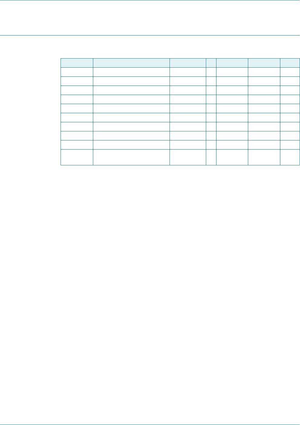
10. Static characteristics
[1] V
DD
must be lowered to 0.2 V for at least 5 s in order to reset part.
Table 14. Static characteristics
V
DD
= 2.3 V to 5.5 V; V
SS
=0V; T
amb
=
40
C to +85
C; unless otherwise specified.
Symbol Parameter Conditions Min Typ Max Unit
Supplies
V
DD
supply voltage 2.3 - 5.5 V
I
DD
supply current Operating mode; V
DD
= 5.5 V; no load;
f
SCL
= 100 kHz
- 135 200 A
I
stb
standby current Standby mode; V
DD
= 5.5 V; no load;
V
I
=V
SS
; f
SCL
= 0 kHz; I/O = inputs
-1.11.5mA
Standby mode; V
DD
= 5.5 V; no load;
V
I
=V
DD
; f
SCL
= 0 kHz; I/O = inputs
-0.251A
V
POR
power-on reset voltage
[1]
no load; V
I
=V
DD
or V
SS
-1.72.2V
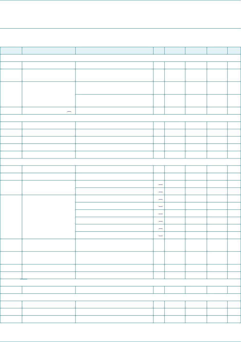
Input SCL; input/output SDA
V
IL
LOW-level input voltage 0.5 - +0.3V
DD
V
V
IH
HIGH-level input voltage 0.7V
DD
-5.5V
I
OL
LOW-level output current V
OL
=0.4V 3 - - mA
I
L
leakage current V
I
=V
DD
=V
SS
1- +1A
C
i
input capacitance V
I
=V
SS
- 6 10 pF
I/Os
V
IL
LOW-level input voltage 0.5 - +0.3V
DD
V
V
IH
HIGH-level input voltage 0.7V
DD
-5.5V
I
OL
LOW-level output current V
DD
= 2.3 V to 5.5 V; V
OL
=0.5V
[2]
8 (8 to 20) - mA
V
DD
= 2.3 V to 5.5 V; V
OL
=0.7V
[2]
10 (10to24) - mA
V
OH
HIGH-level output voltage I
OH
= 8mA; V
DD
=2.3V
[3]
1.8 - - V
I
OH
= 10 mA; V
DD
=2.3V
[3]
1.7 - - V
I
OH
= 8mA; V
DD
=3.0V
[3]
2.6 - - V
I
OH
= 10 mA; V
DD
=3.0V
[3]
2.5 - - V
I
OH
= 8mA; V
DD
=4.75V
[3]
4.1 - - V
I
OH
= 10 mA; V
DD
=4.75V
[3]
4.0 - - V
I
LIH
HIGH-level input leakage
current
V
DD
=5.5V; V
I
=V
DD
-- 1A
I
LIL
LOW-level input leakage
current
V
DD
=5.5V; V
I
=V
SS
-- 100 A
C
i
input capacitance - 3.7 5 pF
C
o
output capacitance - 3.7 5 pF
Interrupt INT
I
OL
LOW-level output current V
OL
=0.4V 3 - - mA
Select inputs A0, A1, A2
V
IL
LOW-level input voltage 0.5 - +0.3V
DD
V
V
IH
HIGH-level input voltage 0.7V
DD
-5.5V
I
LI
input leakage current 1- +1A