PCA9555 All information provided in this document is subject to legal disclaimers. © NXP Semiconductors N.V. 2017. All rights reserved.
Product data sheet Rev. 10 — 8 November 2017 19 of 34
NXP Semiconductors
PCA9555
16-bit I
2
C-bus and SMBus I/O port with interrupt
[2] Each I/O must be externally limited to a maximum of 25 mA and each octal (IO0_0 to IO0_7 and IO1_0 to IO1_7) must be limited to a
maximum current of 100 mA for a device total of 200 mA.
[3] The total current sourced by all I/Os must be limited to 160 mA.
(1) I
OH
= 8mA
(2) I
OH
= 10 mA
(1) I
OH
= 8mA
(2) I
OH
= 10 mA
Fig 19. V
OH
maximum Fig 20. V
OH
minimum
V
DD
= 5.5 V; V
I/O
= 5.5 V; A2, A1, A0 set to logic 0.
(1) T
amb
= 40 C
(2) T
amb
=+25C
(3) T
amb
=+85C
Fig 21. I
DD
versus number of I/Os held LOW
2.0
5.0
4.0
3.0
6.0
V
OH
(V)
V
DD
(V)
2.7 5.53.6
002aac706
(1)
(2)
2.5
3.5
4.5
V
OH
(V)
1.5
V
DD
(V)
2.3 4.753.0
002aac707
(1)
(2)
0
1.2
0.8
0.4
1.6
I
DD
(mA)
number of I/Os
002aac705
all 1s all 0sone 0 three 0s
(1)
(2)
(3)
PCA9555 All information provided in this document is subject to legal disclaimers. © NXP Semiconductors N.V. 2017. All rights reserved.
Product data sheet Rev. 10 — 8 November 2017 20 of 34
NXP Semiconductors
PCA9555
16-bit I
2
C-bus and SMBus I/O port with interrupt
11. Dynamic characteristics
[1] t
VD;ACK
= time for acknowledgement signal from SCL LOW to SDA (out) LOW.
[2] t
VD;DAT
= minimum time for SDA data out to be valid following SCL LOW.
[3] C
b
= total capacitance of one bus line in pF.
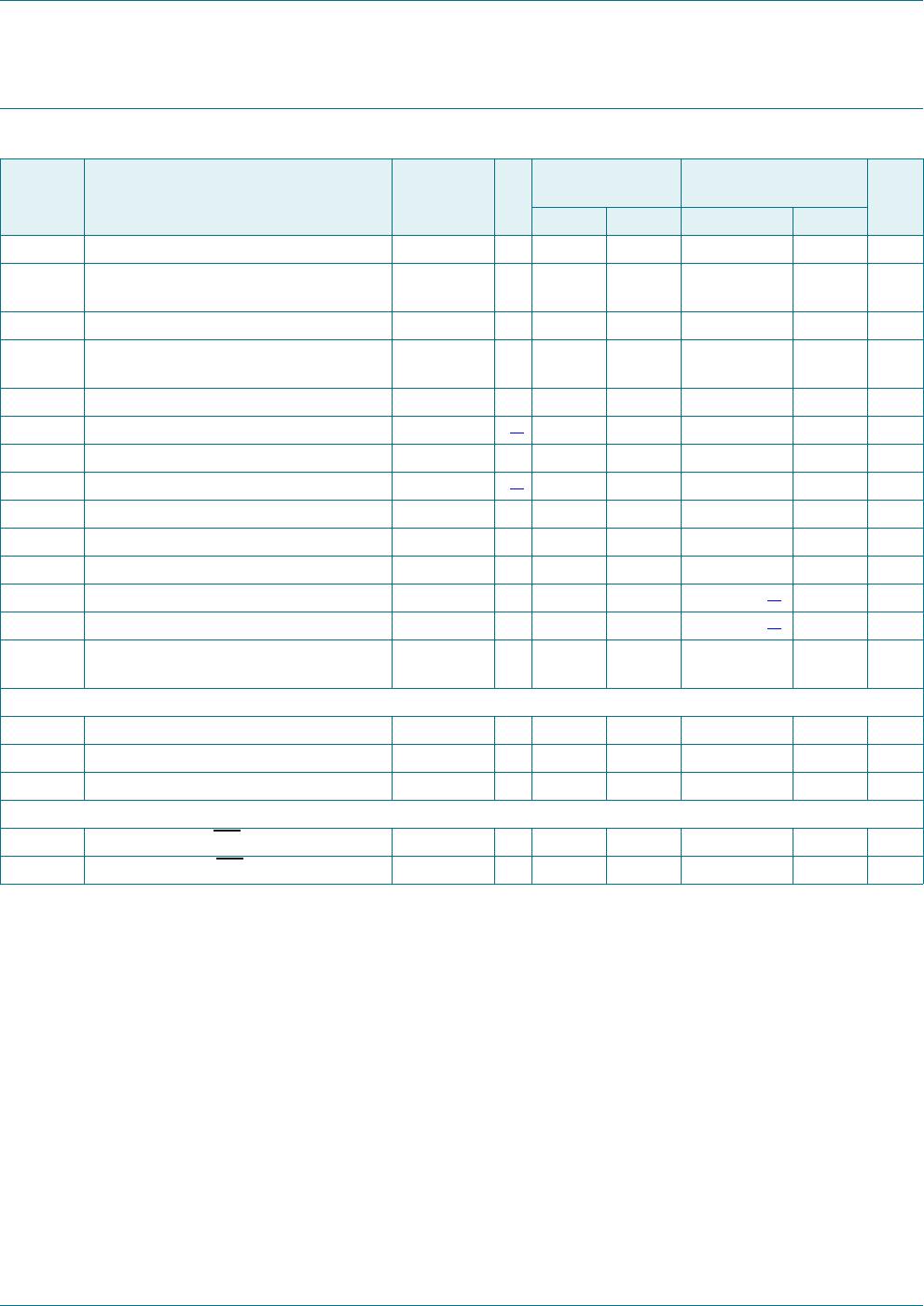
Table 15. Dynamic characteristics
Symbol Parameter Conditions Standard-mode
I
2
C-bus
Fast-mode I
2
C-bus Unit
Min Max Min Max
f
SCL
SCL clock frequency 0 100 0 400 kHz
t
BUF
bus free time between a STOP and
START condition
4.7 - 1.3 - s
t
HD;STA
hold time (repeated) START condition 4.0 - 0.6 - s
t
SU;STA
set-up time for a repeated START
condition
4.7 - 0.6 - s
t
SU;STO
set-up time for STOP condition 4.0 - 0.6 - s
t
VD;ACK
data valid acknowledge time
[1]
0.3 3.45 0.1 0.9 s
t
HD;DAT
data hold time 0 - 0 - ns
t
VD;DAT
data valid time
[2]
300 - 50 - ns
t
SU;DAT
data set-up time 250 - 100 - ns
t
LOW
LOW period of the SCL clock 4.7 - 1.3 - s
t
HIGH
HIGH period of the SCL clock 4.0 - 0.6 - s
t
f
fall time of both SDA and SCL signals - 300 20 + 0.1C
b
[3]
300 ns
t
r
rise time of both SDA and SCL signals - 1000 20 + 0.1C
b
[3]
300 ns
t
SP
pulse width of spikes that must be
suppressed by the input filter
- 50 - 50 ns
Port timing
t
v(Q)
data output valid time - 200 - 200 ns
t
su(D)
data input set-up time 150 - 150 - ns
t
h(D)
data input hold time 1 - 1 - s
Interrupt timing
t
v(INT_N)
valid time on pin INT -4 - 4s
t
rst(INT_N)
reset time on pin INT -4 - 4s
PCA9555 All information provided in this document is subject to legal disclaimers. © NXP Semiconductors N.V. 2017. All rights reserved.
Product data sheet Rev. 10 — 8 November 2017 21 of 34
NXP Semiconductors
PCA9555
16-bit I
2
C-bus and SMBus I/O port with interrupt
12. Test information
Fig 22. Definition of timing on the I
2
C-bus
t
SP
t
BUF
t
HD;STA
PP S
t
LOW
t
r
t
HD;DAT
t
f
t
HIGH
t
SU;DAT
t
SU;STA
Sr
t
HD;STA
t
SU;STO
SDA
SCL
002aaa986
0.7 × V
DD
0.3 × V
DD
0.7 × V
DD
0.3 × V
DD
R
L
= load resistor.
C
L
= load capacitance includes jig and probe capacitance.
R
T
= termination resistance should be equal to the output impedance of Z
o
of the pulse generators.
Fig 23. Test circuitry for switching times
Fig 24. Load circuit
PULSE
GENERATOR
V
O
C
L
50 pF
R
L
500 Ω
002aab284
R
T
V
I
V
DD
DUT
V
DD
open
GND
C
L
50 pF
002aac226
R
L
500 Ω
from output under test
2V
DD
open
GND
S1
R
L
500 Ω

PCA9555PW,118

Mfr. #:
Manufacturer:
NXP Semiconductors
Description:
Interface - I/O Expanders 16-BIT I2C FM TP GPIO INT PU
Lifecycle:
New from this manufacturer.
Delivery:
DHL FedEx Ups TNT EMS
Payment:
T/T Paypal Visa MoneyGram Western Union