CS5521/22/23/24/28
10 DS317F8
DYNAMIC CHARACTERISTICS
RECOMMENDED OPERATING CONDITIONS
(AGND, DGND = 0 V; See Note 20.)
Notes: 20. All voltages with respect to ground.
ABSOLUTE MAXIMUM RATINGS (AGND, DGND = 0 V; See Note 20.)
Notes: 21. No pin should go more negative than NBV - 0.3 V.
22. Applies to all pins including continuous overvoltage conditions at the analog input (AIN) pins.
23. Transient current of up to 100 mA will not cause SCR latch-up. Maximum input current for a power
supply pin is ±50 mA.
24. Total power dissipation, including all input currents and output currents.
WARNING: Operation at or beyond these limits may result in permanent damage to the device.
Normal operation is not guaranteed at these extremes.
Parameter Symbol Ratio Unit
Modulator Sampling Frequency f
s
XIN/4 Hz
Filter Settling Time to 1/2 LSB (Full-scale Step) t
s
1/f
out
s
Parameter Symbol Min Typ Max Unit
DC Power Supplies Positive Digital
Positive Analog
VD+
VA+
2.7
4.75
5.0
5.0
5.25
5.25
V
V
Analog Reference Voltage (VREF+) - (VREF-) VRef
diff
1.0 2.5 VA+ V
Negative Bias Voltage NBV -1.8 -2.1 -2.5 V
Parameter Symbol Min Typ Max Unit
DC Power Supplies (Note 21)
Positive Digital
Positive Analog
VD+
VA+
-0.3
-0.3
-
-
+6.0
+6.0
V
V
Negative Bias Voltage Negative Potential NBV +0.3 -2.1 -3.0 V
Input Current, Any Pin Except Supplies (Note 22 and 23) I
IN
--±10mA
Output Current I
OUT
--±25mA
Power Dissipation (Note 24) PDN - - 500 mW
Analog Input Voltage VREF pins
AIN Pins
V
INR
V
INA
NBV -0.3
NBV -0.3
-
-
(VA+) + 0.3
(VA+) + 0.3
V
V
Digital Input Voltage V
IND
-0.3 - (VD+) + 0.3 V
Ambient Operating Temperature T
A
-40 - 85 °C
Storage Temperature T
stg
-65 - 150 °C
CS5521/22/23/24/28
DS317F8 11
SWITCHING CHARACTERISTICS (T
A
= 25° C; VA+ = 5 V ±5%; VD+ = 3.0 V ±10% or 5 V ±5%;
Levels: Logic 0 = 0 V, Logic 1 = VD+; C
L
= 50 pF.))
Notes: 25. Device parameters are specified with a 32.768 kHz clock; however, clocks up to 200 kHz
(CS5522/24/28) or 130 kHz (CS5521/23) can be used for increased throughput.
26. Specified using 10% and 90% points on waveform of interest. Output loaded with 50 pF.
27. Oscillator start-up time varies with crystal parameters. This specification does not apply when using an
external clock source.
28. Applicable when SCLK is continuously running.
Specifications are subject to change without notice.
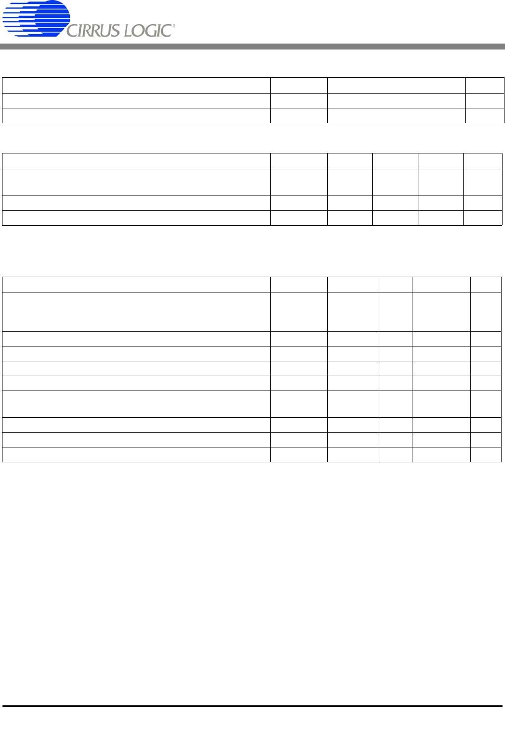
Parameter Symbol Min Typ Max Unit
Master Clock Frequency (Note 25)
External Clock or Internal Oscillator (CS5522/24/28)
(CS5521/23)
XIN
30
30
32.768
32.768
200
130
kHz
kHz
Master Clock Duty Cycle 40 - 60 %
Rise Times (Note 26)
Any Digital Input Except SCLK
SCLK
Any Digital Output
t
rise
-
-
-
-
-
50
1.0
100
-
µs
µs
ns
Fall Times (Note 26)
Any Digital Input Except SCLK
SCLK
Any Digital Output
t
fall
-
-
-
-
-
50
1.0
100
-
µs
µs
ns
Start-up
Oscillator Start-up Time XTAL = 32.768 kHz (Note 27) t
ost
-500-ms
Serial Port Timing
Serial Clock Frequency SCLK 0 - 2 MHz
SCLK Falling to CS
Falling for continuous running SCLK
(Note 28)
t
0
100 - - ns
Serial Clock Pulse Width High
Pulse Width Low
t
1
t
2
250
250
-
-
-
-
ns
ns
SDI Write Timing
CS
Enable to Valid Latch Clock t
3
50 - - ns
Data Set-up Time prior to SCLK rising t
4
50 - - ns
Data Hold Time After SCLK Rising t
5
100 - - ns
SCLK Falling Prior to CS
Disable t
6
100 - - ns
SDO Read Timing
CS
to Data Valid t
7
--150ns
SCLK Falling to New Data Bit t
8
--150ns
CS
Rising to SDO Hi-Z t
9
--150ns
CS5521/22/23/24/28
12 DS317F8
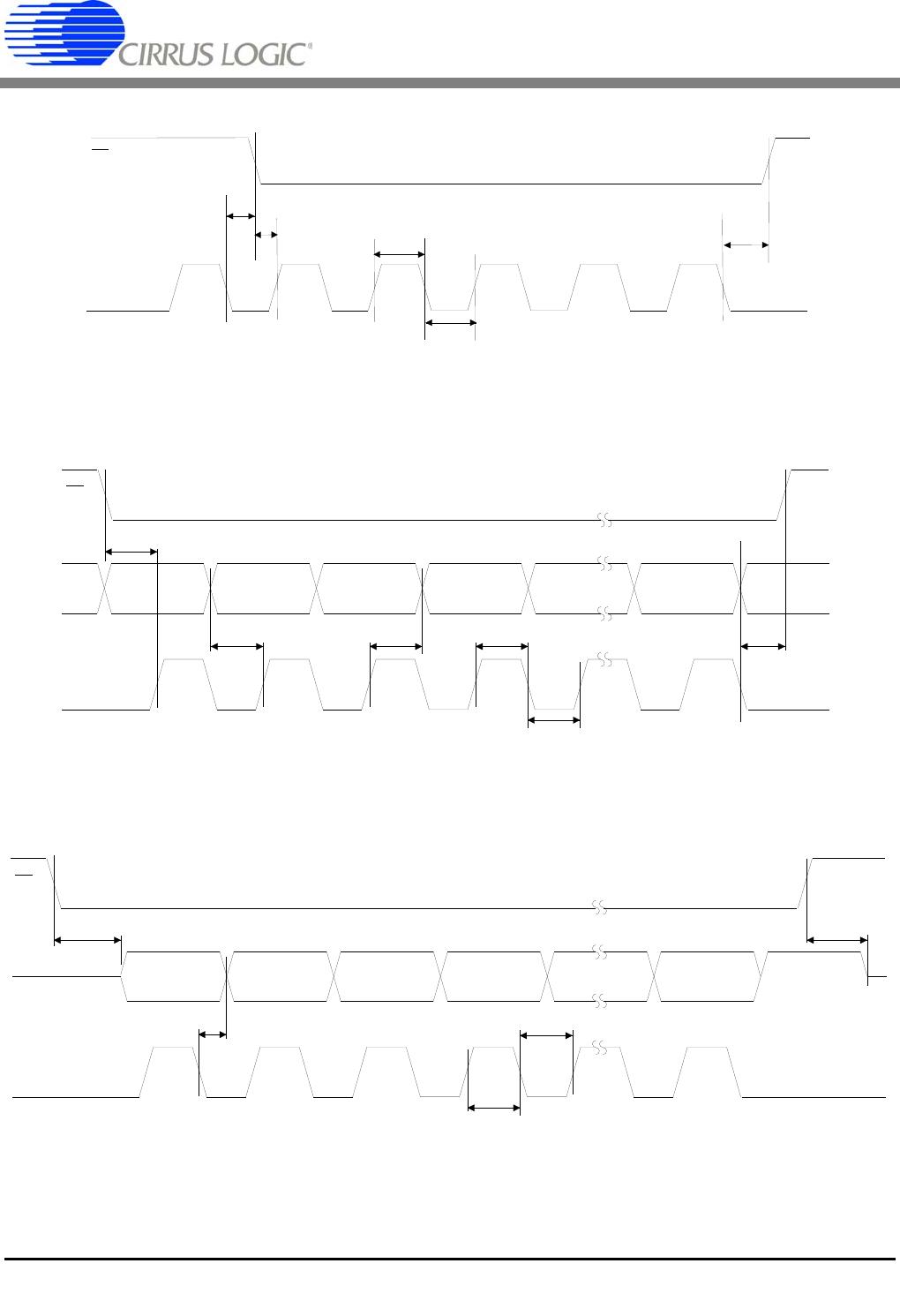
CS
SCLK
t
0
t
2
t
1
t
3
t
6
Figure 1. Continuous Running SCLK Timing (Not to Scale)
CS
SCLK
MSB
MSB-1 LSBSDI
t
3
t
4
t
5
t
1
t
2
t
6
Figure 2. SDI Write Timing (Not to Scale)
CS
SCLK
MSB
MSB-1 LSB
SDO
t
7
t
8
t
1
t
2
t
9
Figure 3. SDO Read Timing (Not to Scale)

CS5522-ASZ

Mfr. #:
Manufacturer:
Cirrus Logic
Description:
Analog to Digital Converters - ADC 2-Ch 24-Bit Delta Sigma ADC
Lifecycle:
New from this manufacturer.
Delivery:
DHL FedEx Ups TNT EMS
Payment:
T/T Paypal Visa MoneyGram Western Union