CS5521/22/23/24/28
DS317F8 7
TYPICAL RMS NOISE, CS5521/23 (Notes 10 and 11)
Notes: 10. Wideband noise aliased into the baseband. Referred to the input. Typical values shown for 25° C.
11. To estimate Peak-to-Peak Noise, multiply RMS noise by 6.6 for all ranges and output rates.
12. For input ranges <100 mV and output rates 60 Sps, 16.384 kHz chopping frequency is used.
TYPICAL NOISE FREE RESOLUTION (BITS), CS5521/23 (Note 13)
Notes: 13. For bipolar mode, the number of bits of Noise Free Resolution is LOG((2XInput Range)/(6.6xRMS
Noise))/LOG(2) rounded to the nearest bit. For unipolar mode, the number of bits of Noise Free
Resolution is LOG((Input Range)/(6.6xRMS Noise))/LOG(2) rounded to the nearest bit. Also, the
CS5521/23’s output conversions are 16 bits. Noise free Resolution numbers are based upon
VREF = 2.5 V and XIN = 32.768 kHz. The values will be affected directly by changes in VREF, but the
effects due to changes in the XIN frequency will be minor.
Output Rate
(Sps)
-3 dB Filter
Frequency
Input Range, (Bipolar/Unipolar Mode)
25 mV 55 mV 100 mV 1 V 2.5 V 5 V
1.88 1.64 90 nV 148 nV 220 nV 1.8 µV 3.9 µV 7.8 µV
3.76 3.27 122 nV 182 nV 310 nV 2.6 µV 5.7 µV 11.3 µV
7.51 6.55 180 nV 267 nV 435 nV 3.7 µV 8.5 µV 18.1 µV
15.0 12.7 280 nV 440 nV 810 nV 5.7 µV 14 µV 28 µV
30.0 25.4 580 nV 1.1 µV 2.1 µV 18.2 µV 48 µV 96 µV
61.6 (Note 12) 50.4 2.6 µV 4.9 µV 8.5 µV 92 µV 238 µV 390 µV
84.5 (Note 12) 70.7 11 µV 27 µV 43 µV 458 µV 1.1 mV 2.4 mV
101.1 (Note 12) 84.6 41 µV 72 µV 130 µV 1.2 mV 3.4 mV 6.7 mV
Output Rate
(Sps)
-3 dB Filter
Frequency
Input Range, (Bipolar Mode)
25 mV 55 mV 100 mV 1 V 2.5 V 5 V
1.88 1.64 16 16 16 16 16 16
3.76 3.27 16 16 16 16 16 16
7.51 6.55 15 16 16 16 16 16
15.0 12.7 15 15 15 16 16 16
30.0 25.4 14 14 14 14 14 14
61.6 (Note 12) 50.4 12 12 12 12 12 12
84.5 (Note 12)70.7999999
101.1 (Note 12)84.6888888
CS5521/22/23/24/28
8 DS317F8
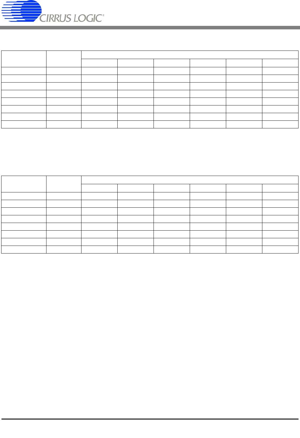
TYPICAL RMS NOISE, CS5522/24/28 (Notes 14 and 15)
Notes: 14. Wideband noise aliased into the baseband. Referred to the input. Typical values shown for 25° C.
15. To estimate Peak-to-Peak Noise, multiply RMS noise by 6.6 for all ranges and output rates.
16. For input ranges <100 mV and output rates 60 Sps, 16.384 kHz chopping frequency is used.
TYPICAL NOISE FREE RESOLUTION (BITS), CS5522/24/28 (Note 17)
Notes: 17. For bipolar mode, the number of bits of Noise Free Resolution is LOG((2XInput Range)/(6.6xRMS
Noise))/LOG(2) rounded to the nearest bit. For unipolar mode, the number of bits of Noise Free
Resolution is LOG((Input Range)/(6.6xRMS Noise))/LOG(2) rounded to the nearest bit. Also, the
CS5522/24/28’s output conversions are 24 bits. Noise free Resolution numbers are based upon
VREF = 2.5 V and XIN = 32.768 kHz. The values will be affected directly by changes in VREF, but the
effects due to changes in the XIN frequency will be minor.
Output Rate
(Sps)
-3 dB Filter
Frequency
Input Range, (Bipolar/Unipolar Mode)
25 mV 55 mV 100 mV 1 V 2.5 V 5 V
1.88 1.64 90 nV 95 nV 140 nV 1.5 µV 3 µV 6 µV
3.76 3.27 110 nV 130 nV 190 nV 2 µV 4 µV 8 µV
7.51 6.55 170 nV 200 nV 275 nV 2.5 µV 6 µV 11.5 µV
15.0 12.7 250 nV 330 nV 580 nV 4.5 µV 10 µV 20 µV
30.0 25.4 500 nV 1 µV 1.5 µV 16 µV 45 µV 85 µV
61.6 (Note 16) 50.4 2 µV 4 µV 8 µV 72 µV 195 µV 350 µV
84.5 (Note 16) 70.7 10 µV 20 µV 35 µV 340 µV 900 µV 2 mV
101.1 (Note 16) 84.6 30 µV 60 µV 105 µV 1.1 mV 3 mV 5.3 mV
Output Rate
(Sps)
-3 dB Filter
Frequency
Input Range, (Bipolar Mode)
25 mV 55 mV 100 mV 1 V 2.5 V 5 V
1.88 1.64 16 17 18 18 18 18
3.76 3.27 16 17 17 17 18 18
7.51 6.55 15 16 17 17 17 17
15.0 12.7 15 16 16 16 16 16
30.0 25.4 14 14 14 14 14 14
61.6 (Note 16) 50.4 12 12 12 12 12 12
84.5 (Note 16) 70.7 10 10 10 10 10 10
101.1 (Note 16)84.6888888
CS5521/22/23/24/28
DS317F8 9
5 V DIGITAL CHARACTERISTICS (T
A
= 25° C; VA+, VD+ = 5 V ±5%; GND = 0;
See Notes 2 and 18.))
Notes: 18. All measurements performed under static conditions.
19. I
out
= -100 µA unless stated otherwise. (V
OH
= 2.4 V @ I
out
= -40 µA.)
3 V DIGITAL CHARACTERISTICS (T
A
= 25° C; VA+ = 5 V ±5%; VD+ = 3.0 V ±10%; GND = 0;
See Notes 2 and 18.)
Parameter Symbol Min Typ Max Unit
High-level Input Voltage All Pins Except XIN and SCLK
XIN
SCLK
V
IH
0.6 VD+
(VD+)-0.5
(VD+) - 0.45
-
-
-
-
-
-
V
V
V
Low-level Input Voltage All Pins Except XIN and SCLK
XIN
SCLK
V
IL
-
-
-
-
-
-
0.8
1.5
0.6
V
V
V
High-level Output Voltage
All Pins Except CPD and SDO (Note 19)
CPD, I
out
= -4.0 mA
SDO, I
out
= -5.0 mA
V
OH
(VA+) - 1.0
(VD+) - 1.0
(VD+) - 1.0
-
-
-
-
-
-
V
V
V
Low-level Output Voltage
All Pins Except CPD and SDO, I
out
= 1.6 mA
CPD, I
out
= 2 mA
SDO, I
out
= 5.0 mA
V
OL
-
-
-
-
-
-
0.4
0.4
0.4
V
V
V
Input Leakage Current I
in
1±10µA
3-state Leakage Current I
OZ
--±10µA
Digital Output Pin Capacitance C
out
-9-pF
Parameter Symbol Min Typ Max Unit
High-level Input Voltage All Pins Except XIN and SCLK
XIN
SCLK
V
IH
0.6 VD+
(VD+)-0.5
(VD+) - 0.45
-
-
-
-
-
-
V
V
V
Low-level Input Voltage All Pins Except XIN and SCLK
XIN
SCLK
V
IL
-
-
-
-
-
-
0.16 VD+
0.3
0.6
V
V
V
High-level Output Voltage
All Pins Except CPD and SDO, I
out
= -400 µA
CPD, I
out
= -4.0 mA
SDO, I
out
= -5.0 mA
V
OH
(VA+) - 0.3
(VD+) - 1.0
(VD+) - 1.0
-
-
-
-
-
-
V
V
V
Low-level Output Voltage
All Pins Except CPD and SDO, I
out
= 400 µA
CPD, I
out
= 2 mA
SDO, I
out
= 5.0 mA
V
OL
-
-
-
-
-
-
0.3
0.4
0.4
V
V
V
Input Leakage Current I
in
1±10µA
3-state Leakage Current I
OZ
--±10µA
Digital Output Pin Capacitance C
out
-9-pF

CS5522-ASZ

Mfr. #:
Manufacturer:
Cirrus Logic
Description:
Analog to Digital Converters - ADC 2-Ch 24-Bit Delta Sigma ADC
Lifecycle:
New from this manufacturer.
Delivery:
DHL FedEx Ups TNT EMS
Payment:
T/T Paypal Visa MoneyGram Western Union