CS5521/22/23/24/28
DS317F8 31
1.3 Calibration
The CS5521/22/23/24/28 offer four different cali-
bration functions including self calibration and sys-
tem calibration. However, after the devices are
reset, the converter is functional and can perform
measurements without being calibrated. In this
case, the converter will utilize the initialized values
of the on-chip registers (Gain = 1.0, Offset = 0.0)
to calculate output words for the ±100 mV range.
Any initial offset and gain errors in the internal cir-
cuitry of the chip will remain.
The gain and offset registers, which are used for
both self and system calibration, are used to set the
zero and full-scale points of the converter’s transfer
function. One LSB in the offset register is 2
-24
pro-
portion of the input span when the gain register is
set to 1.0 decimal (bipolar span is 2 times the uni-
polar span). The MSB in the offset register deter-
mines if the offset to be trimmed is positive or
negative (0 positive, 1 negative). The converter can
typically trim ±50 percent of the input span. The
gain register spans from 0 to (4 - 2
-22
). The decimal
equivalent meaning of the gain register is:
where the binary numbers have a value of either
zero or one (b
0
corresponds to bit MSB-1, N=22).
Refer to Table 5 for details.
The offset and gain calibration steps each take one
conversion cycle to complete. At the end of the cal-
ibration step, SDO falls to indicate that the calibra-
tion has finished.
1.3.1 Self Calibration
The CS5521/22/23/24/28 offer both self-offset and
self-gain calibrations. For self calibration of offset
in the 25 mV, 55 mV, and 100 mv ranges, the con-
verters internally tie the inputs of the instrumenta-
tion amplifier together and route them to the AIN-
pin as shown in Figure 11 (in the CS5528 they are
routed to AGND). For proper self-calibration of
Table 5. Offset and Gain Registers
Offset Register
One LSB represents 2
-24
proportion of the input span when gain register is set to 1.0 decimal (bipolar span is
2 times unipolar span)
Offset and data word bits align by MSB (bit MSB-4 of offset register changes bit MSB-4 of data)
Gain Register
The gain register span is from 0 to (4-2
-22
). After Reset the (MSB-1) bit is 1, all other bits are 0.
MSB LSB
Register
Sign
2
-2
2
-3
2
-4
2
-5
2
-6
2
-19
2
-20
2
-21
2
-22
2
-23
2
-24
Reset (R) 000000 000000
MSB LSB
Register
2
1
2
0
2
-1
2
-2
2
-3
2
-4
2
-17
2
-18
2
-19
2
-20
2
-21
2
-22
Reset (R) 010000 000000
Db
MSB
2
1
b(
0
2
0
b
1
2
1
b
N
2
N
)++++ b
MSB
2
1
b
i
2
i
i 0=
N
+==
CS5521/22/23/24/28
32 DS317F8
offset to occur in the 25 mV, 55 mV, and 100 mV
ranges, the AIN- pin must be at the proper com-
mon-mode voltage as specified in ‘Common Mode
+Signal AIN+/-’ specification in the Analog Input
section (if AIN- = 0 V, NBV must be between -
1.8 V to -2.5 V). For self calibration of offset in the
1.0 V, 2.5 V, and 5 V ranges, the inputs of the mod-
ulator are connected together and then routed to the
VREF- pin as shown in Figure 12.
For self calibration of gain, the differential inputs
of the modulator are connected to VREF+ and
VREF- as shown in Figure 13. For any input range
other than the 2.5 V range, the converter’s gain er-
ror can not be completely calibrated out when using
self calibration. This is due to the lack of an accu-
rate full-scale voltage internal to the chips. The
2.5 V range is an exception because the external
reference voltage is 2.5 V nominal and is used as
the full-scale voltage. In addition, when self cali-
bration of gain is performed in the 25 mV, 55 mV,
and 100 mV input ranges, the instrumentation am-
plifier’s gain is not calibrated. These two factors
can leave the converters with a gain error of up to
±20% after self calibration of gain. Therefore, a
system gain calibration is required to get better ac-
curacy, except for the 2.5 V range.
1.3.2 System Calibration
For the system calibration functions, the user must
supply the calibration signals to the converter which
represent ground and full scale. When a system offset
calibration is performed, a ground-referenced signal
must be applied to the converters. See
Figures 14 and 15.
As shown in Figures 16 and 17, the user must input
a signal representing the positive full-scale point to
AIN+
AIN-
S1
OPEN
S2
CLOSED
+
-
X20
+
-
AIN+
AIN-
S1
OPEN
+
-
X20
+
-
S2
OPEN
S4
CLOSED
VREF-
S3
CLOSED
Figure 12. Self Calibration of Offset (High Ranges)
AIN+
AIN-
OPEN
+
-
X20
+
-
OPEN
CLOSED
VREF+
CLOSED
VREF-
+
-
Reference
Figure 13. Self Calibration of Gain (All Ranges)
+
-
X20
+
-
External
Connections
0V
+
-
AIN+
AIN-
CM
+
-
Figure 14. System Calibration of Offset (Low Ranges)
CS5521/22/23/24/28
DS317F8 33
perform a system gain calibration. In either case,
the calibration signals must be within the specified
calibration limits for each specific calibration step
(refer to the ‘System Calibration Specifications’ in
ANALOG CHARACTERISTICS). If a system gain
calibration is performed the following conditions
must be met:
1) Full-scale input must not saturate the 20X in-
strumentation amplifier, if the calibration is on
an input range where the instrumentation am-
plifier is involved.
2) The 1’s density of the modulator must not be
greater than 80 percent (the input to the ΔΣ
modulator must not exceed the maximum input
which Table 1 specifies).
3) The input must not be so small, relative to the
range chosen, that the resulting gain register’s
content, decoded in decimal, exceeds
3.9999998 (see the discussion of operating lim-
its on input span under the Analog Input and
Limitations in Calibration Range sections).
This requires the full-scale input voltage to the
modulator to be at least 25 percent of the nom-
inal value.
The converter’s input ranges were chosen to guar-
antee gain calibration accuracy to 1 LSB
16
or 16
LSB
24
when system gain calibration is performed.
This is useful when a user wants to manually scale
the full-scale range of the converter and maintain
accuracy. For example, if a gain calibration is per-
formed with a 2.5 V full-scale voltage and a 1.25 V
input range is desired, the user can read the con-
tents of the gain register, shift the register contents
left by 1 bit, and then write the result back to the
gain register. This multiplies the gain by 2.
Assuming a system can provide two known voltag-
es, the following equations allow the user to manu-
ally compute the calibration register’s values based
on two uncalibrated conversions (see note). The
offset and gain calibration registers are used to ad-
just a typical conversion as follows:
Rc = (Ru + Co) * Cg / 2
22
.
Calibration can be performed using the following
equations:
Co = (Rc0/G - Ru0)
Cg = 2
22
* G
where G = (Rc1 - Rc0)/(Ru1-Ru0).
Note: Uncalibrated conversions imply that the gain and off-
set registers are at default {gain register = 0x400000
(Hex) and offset register = 0x000000 (Hex)}.
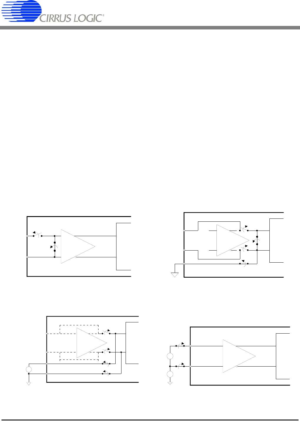
+
-
X20
+
-
External
Connections
+
-
AIN+
AIN-
CM
+
-
0V
Figure 15. System Calibration of Offset (High Ranges)
+
-
X20
+
-
External
Connections
Full Scale
+
-
AIN+
AIN-
CM
+
-
Figure 16. System Calibration of Gain (Low Ranges)
+
-
X20
+
-
External
Connections
Full Scale
+
-
AIN+
AIN-
CM
+
-
Figure 17. System Calibration of Gain (High Ranges)

CS5522-ASZ

Mfr. #:
Manufacturer:
Cirrus Logic
Description:
Analog to Digital Converters - ADC 2-Ch 24-Bit Delta Sigma ADC
Lifecycle:
New from this manufacturer.
Delivery:
DHL FedEx Ups TNT EMS
Payment:
T/T Paypal Visa MoneyGram Western Union