CS5521/22/23/24/28
DS317F8 19
1.2.2 Command Register Quick Reference
D7(MSB)D6D5D4D3D2D1D0
CB CS2 CS1 CS0 R/W
RSB2 RSB1 RSB0
BIT NAME VALUE FUNCTION
D7 Command Bit, CB 0
1
Must be logic 0 for these commands.
See table below.
D6-D4 Channel Select Bits,
CSB2-CSB0
000
.
.
111
CS2-CS0 provide the address of one of the eight physical
channels. These bits are used to access the calibration regis-
ters associated with respective channels.
Note: These bits are ignored when reading the data register.
D3 Read/Write
, R/W
0
1
Write to selected register.
Read from selected register.
D2-D0 Register Select Bit,
RSB2-RSB0
000
001
010
011
101
110
111
Reserved
Offset Register
Gain Register
Configuration Register
Channel Set-up Registers
- register is 48-bits long for CS5521/22
- register is 96-bits long for CS5523/24
- register is 192-bits long for CS5528
Reserved
Reserved
D7(MSB)D6D5D4D3D2D1D0
CB CSRP3 CSRP2 CSRP1 CSRP0 CC2 CC1 CC0
BIT NAME VALUE FUNCTION
D7 Command Bit, CB 0
1
See table above.
Must be logic 1 for these commands.
D6-D3 Channel Pointer Bits,
CSRP3-CSRP0
0000
.
.
.
1111
These bits are used as pointers to the Setups.
Note: The MC bit, must be logic 0 for these bits to take effect.
When MC = 1, these bits are ignored. The LP, MC, and RC
bits in the configuration register are ignored during calibra-
tion.
D2-D0 Conversion/Calibration
Bits, CC2-CC0
000
001
010
011
100
101
110
111
Normal Conversion
Self-Offset Calibration
Self-Gain Calibration
Reserved
Reserved
System-Offset Calibration
System-Gain Calibration
Reserved
Table 2. Command Register Quick Reference
CS5521/22/23/24/28
20 DS317F8
1.2.3 Command Register Descriptions
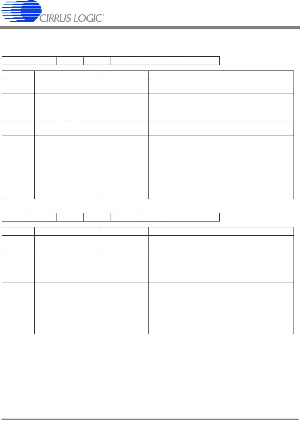
READ/WRITE INDIVIDUAL OFFSET CALIBRATION REGISTER
Function
: These commands are used to access each offset register separately. CS1 - CS0 decode the
registers accessed.
R/W
(Read/Write)
0 Write to selected register.
1 Read from selected register.
CS[2:0] (Channel Select Bits)
000 Offset Register 1(All devices)
001 Offset Register 2 (All devices)
010 Offset Register 3 (CS5523/24/28 only)
011 Offset Register 4 (CS5523/24/28 only)
100 Offset Register 5 (CS5528 only)
101 Offset Register 6 (CS5528 only)
110 Offset Register 7 (CS5528 only)
111 Offset Register 8 (CS5528 only)
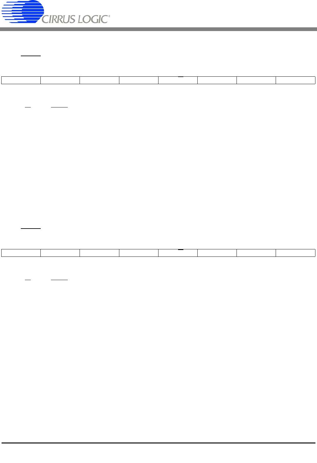
READ/WRITE INDIVIDUAL GAIN REGISTER
Function
: These commands are used to access each gain register separately. CS1 - CS0 decode the reg-
isters accessed.
R/W
(Read/Write)
0 Write to selected register.
1 Read from selected register.
CS[2:0] (Channel Select Bits)
000 Gain Register 1(All devices)
001 Gain Register 2 (All devices)
010 Gain Register 3 (CS5523/24/28 only)
011 Gain Register 4 (CS5523/24/28 only)
100 Gain Register 5 (CS5528 only)
101 Gain Register 6 (CS5528 only)
110 Gain Register 7 (CS5528 only)
111 Gain Register 8 (CS5528 only)
D7(MSB) D6 D5 D4 D3 D2 D1 D0
0 CS2 CS1 CS0 R/W
001
D7(MSB) D6 D5 D4 D3 D2 D1 D0
0 CS2 CS1 CS0 R/W
010
CS5521/22/23/24/28
DS317F8 21
READ/WRITE CONFIGURATION REGISTER
Function: These commands are used to read from or write to the configuration register.
R/W
(Read/Write)
0 Write to selected register.
1 Read from selected register.
READ/WRITE CHANNEL-SETUP REGISTER(S)
Function
: These commands are used to access the channel-setup registers (CSRs). The number of
CSRs accessed is determined by the device being used and the number of CSRs that are being
accessed (i.e. the depth bits in the configuration register determine the number of levels ac-
cessed). This register is 48-bits long (4 Setups) for the CS5521/22, 96-bits long (8 Setups) for
the CS5523/24, and 192-bits (16 Setups) long for the CS5528.
R/W
(Read/Write)
0 Write to selected register.
1 Read from selected register.
D7(MSB) D6 D5 D4 D3 D2 D1 D0
0000R/W
011
D7(MSB) D6 D5 D4 D3 D2 D1 D0
0000R/W
101

CS5522-ASZ

Mfr. #:
Manufacturer:
Cirrus Logic
Description:
Analog to Digital Converters - ADC 2-Ch 24-Bit Delta Sigma ADC
Lifecycle:
New from this manufacturer.
Delivery:
DHL FedEx Ups TNT EMS
Payment:
T/T Paypal Visa MoneyGram Western Union