CS5521/22/23/24/28
16 DS317F8
mentation amplifier with a gain range setting of
100 mV or less, is typically 100 pA. This is low
enough to permit large external resistors to divide
down a large external signal without significant
loading. Figure 7 illustrates an example circuit. Re-
fer to Application Note 158 for more details on
high-voltage (>5 V) measurement.
1.1.5 Voltage Reference
The CS5521/22/23/24/28 devices are specified for
operation with a 2.5 V reference voltage between
the VREF+ and VREF- pins of the device. For a
single-ended reference voltage, such as the
LT1019-2.5, the reference voltage is input into the
VREF+ pin of the converter and the VREF- pin is
grounded.
The differential voltage between the VREF+ and
VREF- can be any voltage from 1.0 V up to VA+,
however, the VREF+ cannot go above VA+ and the
VREF- pin can not go below NBV.
Figure 8 illustrates the input models for the VREF
pins. The dynamic input current for each of the pins
can be determined from the models shown.
1.2 Overview of ADC Register Structure
and Operating Modes
The CS5521/22/23/24/28 ADCs have an on-chip
controller, which includes a number of user-acces-
sible registers. The registers are used to hold offset
and gain calibration results, configure the chip's
operating modes, hold conversion instructions, and
to store conversion data words. Figure 9 depicts a
block diagram of the on-chip controller’s internal
registers for the CS5523/24.
Each of the converters has 24-bit registers to func-
tion as offset and gain calibration registers for each
channel. The converters with two channels have
two offset and two gain calibration registers, the
converters with four channels have four offset and
four gain calibration registers, and the eight chan-
nel converter has eight offset and eight gain cali-
bration registers. These registers hold calibration
results. The contents of these registers can be read
or written by the user. This allows calibration data
to be off-loaded into an external EEPROM. The
user can also manipulate the contents of these reg-
isters to modify the offset or the gain slope of the
converter.
The converters include a 24-bit configuration reg-
ister of which 17 of the bits are used for setting op-
tions such as the conversion mode, operating power
options, setting the chop clock rate of the instru-
Voltage
Divider
PGIA set for
+
100 mV
±10V
Charge Pump
Regulator
ΔΣ
ADC
PGIA
+5 V
2.5 V
VA+
VREF+
VREF-
VD+
+
-
NBV
V
-2.1 V
+
10
μ
F
0.033
μ
F
CPD
0.1
μ
F
10
Ω
0.1
μ
F
1N4148
1N4148BAT85
Charge Pump
Circuitry
DGND
chop clock = 256 Hz
10 K
Ω
1 M
Ω
Figure 7. Input Ranges Greater than 5 V
VREF
C = 10pF
f = 32.768 kHz
2
φ
Fine
1
V
25mV
i = fV C
os
osn
φ
Coarse
CS5521/22/23/24/28
DS317F8 17
mentation amplifier, and providing a number of
flags which indicate converter operation.
A group of registers, called Channel Set-up Regis-
ters, are also included in the converters. These reg-
isters are used to hold pre-loaded conversion
instructions. Each channel set-up register is 24 bits
wide and holds two 12-bit conversion instructions
(Setups). Upon power-up, these registers can be
initialized by the user’s microcontroller with con-
version instructions. The user can then use bits in
the configuration register to choose a conversion
mode.
Several conversion modes are possible. Using the
single conversion mode, an 8-bit command word
can be written into the serial port. The command in-
cludes pointer bits which ‘point’ to a 12-bit com-
mand in one of the Channel Setup Registers which
is to be executed. The 12-bit commands can be set-
up to perform a conversion on any of the input
channels of the converter. More than one of the 12-
bit Setups can be used for the same analog input
channel. This allows the user to convert on the
same signal with either a different conversion
speed, a different gain range, or any of the other op-
tions available in the Setup Register. The user can
set up the registers to perform conversions using
different conversion options on each of the input
channels.
The ADCs also include multiple-channel conver-
sion capability. User bits in the configuration regis-
ter of the ADCs can be configured to sequence
through the 12-bit command Setups, performing a
conversion according to the content of each 12-bit
Setup. This channel scanning capability can be
configured to run continuously, or to scan through
a specified number of Setup Registers and stop un-
til commanded to continue. In the multiple-channel
scanning modes, the conversion data words are
loaded into an on-chip data FIFO. The converter is-
sues a flag on the SDO pin when a scan cycle is
completed so the user can read the FIFO. More de-
tails are given in the following pages.
Instructions are provided on how to initialize the
converter, perform offset and gain calibrations, and
to configure the converter for the various conver-
sion modes. Each of the bits of the configuration
register and of the Channel Setup Registers is de-
scribed. A list of examples follows the description
section. Table 2 can be used to decode all valid
commands (the first 8 bits into the serial port).
AIN1
AIN2
AIN3
AIN4
4 (24) 4 (24) 4 (12 x 2) 8 x 24
Off 1
Off 2
Off 3
Off 4
Gain 1
Gain 2
Gain 3
Gain 4
Setup 1
Setup 3
Setup 5
Setup 7
Setup 2
Setup 4
Setup 6
Setup 8
DATA
FIFO
SDO
1 x 24
Configuration
Chop Frequency
Multiple Conversions
Depth Pointer
Loop
Read Convert
Powerdown Modes
Flags
Etc.
Latch Outputs
Channel Select
Output Word Rate
PGA Selection
Unipolar/Bipolar
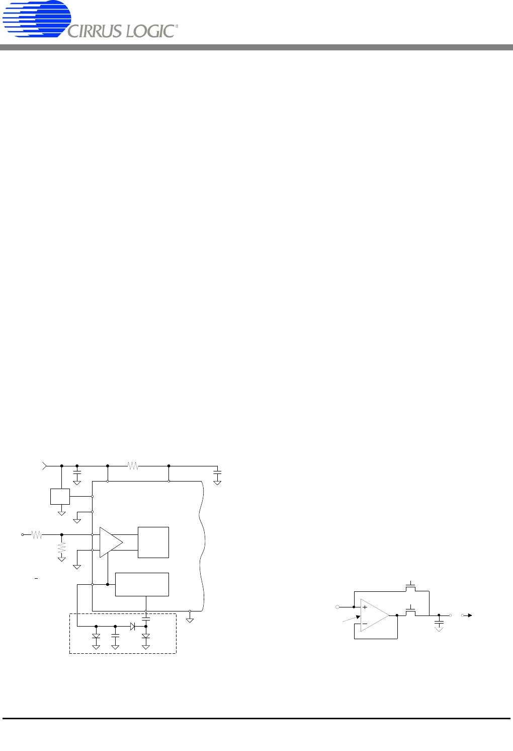
Figure 9. CS5523/24 Register Diagram
CS5521/22/23/24/28
18 DS317F8
1.2.1 System Initialization
After power is first applied to the
CS5521/22/2324/28 devices, the user should wait
for the oscillator to start before attempting to com-
municate with the converter. If a 32.768 kHz crys-
tal is used, this may be 500 milliseconds.
The initialization sequence should be as follows:
Initialize the serial port by sending the port initial-
ization sequence of 15 bytes of all 1's followed by
one byte with the following bit contents '1111 110'.
This sequence places the chip in the command
mode where it waits for a valid command to be
written. The first command should be to perform a
system reset. This is accomplished by writing a
logic 1 to the RS (Reset System) bit in the configu-
ration register. After a reset the RV bit is set until
the configuration register is read. The user must
then write a logic 0 to the RS bit to take the part out
of reset mode. Any other bits written to the config-
uration register at this time will be lost. The con-
figuration register must be written again once RS=
0 to set any other bits to their desired settings.
After a reset, the on-chip registers are initialized to
the following states:
configuration register: 000040(H)
offset registers: 000000(H)
gain registers: 400000(H)
channel setup registers: 000000(H)

CS5522-ASZ

Mfr. #:
Manufacturer:
Cirrus Logic
Description:
Analog to Digital Converters - ADC 2-Ch 24-Bit Delta Sigma ADC
Lifecycle:
New from this manufacturer.
Delivery:
DHL FedEx Ups TNT EMS
Payment:
T/T Paypal Visa MoneyGram Western Union