LTC4417
3
4417f
elecTrical characTerisTics
The l denotes the specifications which apply over the full operating
temperature range, otherwise specifications are at T
A
= 25°C. For all tests, V1 = VS1, V2 = VS2, V3 = VS3. Unless otherwise noted,
V1 = V2 = V3 = V
OUT
= 12V, HYS = GND.
SYMBOL PARAMETER CONDITIONS MIN TYP MAX UNITS
Start-Up
V1-V3,V
OUT
V1 to V3,V
OUT
Operating Supply Range
l
2.5 36 V
I
V1-V3,VOUT(EN)
Total Supply Current with Channels Enabled V1 = 5V, V2 = 12V, V3 = 2.5V, V
OUT
= 4V,
(Notes 3, 4)
l
28 78 µA
I
V1-V3(EN)
Total Supply Current with Channels Disabled V1 = 5V, V2 = 12V, V3 = 2.5V, V
OUT
= EN = 0V,
(Notes 3, 4)
l
31 93 µA
I
V1-V3(SHDN)
Total Supply Current When Shutdown V1 = 5V, V2 = 12V, V3 = 2.5V, V
OUT
= SHDN =
0V, (Notes 3, 4)
l
15.4 84 µA
I
VOUT
V
OUT
Supply Current V1 = 5V, V2 = 12V, V3 = 2.5V, V
OUT
= 4V
l
14 30 µA
I
PRIORITY
Current from Highest V1 to V3 Priority Input
Source (V1)
V1 = 5V, V2 = 12V, V3 = 2.5V, V
OUT
= 4V
V1 = 5V, V2 = 12V, V3 = 2.5V, V
OUT
= EN = 0V
l
l
2.6
20
6
45
µA
µA
I
HIGHEST
Current from Highest V1 to V3 Voltage Input
Source
V1 = 5V, V2 = 12V, V3 = 2.5V, V
OUT
= 4V,
(Note 3, 4)
l
11 72 µA
V1 = 5V, V2 = 12V, V3 = 2.5V, V
OUT
= EN = 0V,
SHDN = 0V, (Note 3, 4)
l
15 80 µA
I
LOWER
Current from V1 to V3 Input Voltage Sources
Lower than V
OUT
V1 = 5V, V2 = 12V, V3 = 2.5V, V
OUT
= 4V
Not Highest Valid Priority
–5 0.2 1 µA
Gate Control
∆V
G
Open (VS – VG) Clamp Voltage V
OUT
= 11V, G1 to G3 = Open
l
5.4 6.2 6.7 V
∆V
G(SOURCE)
Sourcing (VS – VG) Clamp Voltage V
OUT
= 11V, I = –10µA
l
5.8 6.6 7 V
∆V
G(SINK)
Sinking (VS – VG) Clamp Voltage V
OUT
= 11V, I = 10µA
l
4.5 5.2 6 V
∆V
G(OFF)
G1 to G3 Off (VS – VG) Threshold V1 = V2 = V3 = 2.8V, V
OUT
= 2.6V, G1 to G3
Rising Edge
l
0.12 0.35 0.6 V
∆V
G(SLEW,ON)
G1 to G3 Pull-Down Slew Rate V
OUT
= 11V, C
GATE
= 10nF (Note 5)
l
4 9 20 V/µs
∆V
G(SLEW,OFF)
G1 to G3 Pull-Up Slew Rate V
OUT
= 11V, C
GATE
= 10nF (Note 6)
l
7.5 13 22 V/µs
I
G(DN)
G1 to G3 Low Pull-Down Current V
OUT
= 2.6V, V1 to V3 = 2.8V, (G1 to G3) = ∆V
G
+ 300mV
0.8 2 7 µA
R
G(OFF)
G1 to G3 OFF Resistance V
OUT
= 4V, V1 to V3 = 5V, I
G
= –10mA
l
9 16 26 Ω
V
REV
Reverse Voltage Threshold Measure (V1 to V3) – V
OUT
, V
OUT
Falling
l
30 120 200 mV
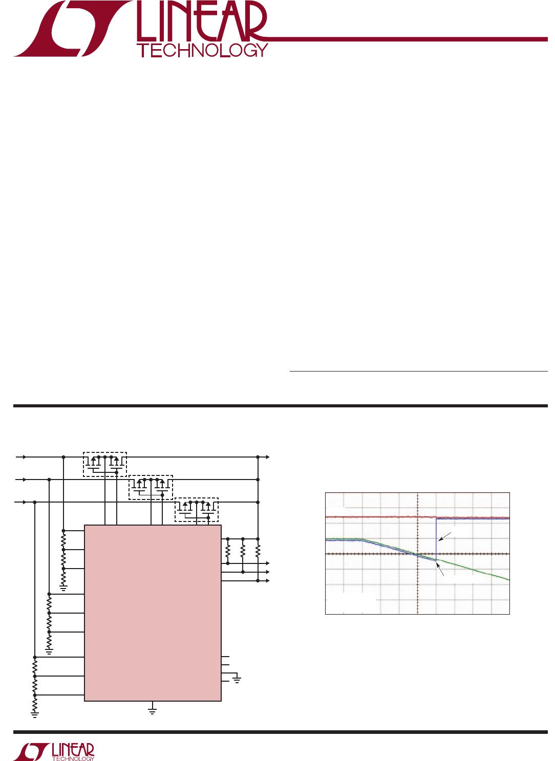
t
G(SWITCHOVER)
Pin Break-Before-Make Time V
OUT
= 11V, C
GATE
= 10nF, (Note 7)
l
0.7 2 3 µs
t
pG(SHDN)
G1 to G3 Turn-Off Delay From SHDN V
OUT
= 11V, Falling Edge SHDN to
(G1 to G3) = (VS1 to VS3) – 3V, C
GATE
= 10nF
l
20 50 100 µs
t
pG(EN,OFF)
G1 to G3 Turn-Off Delay From EN V
OUT
= 11V, Falling EN Edge to
(G1 to G3) = (VS1 to VS3) – 3V, C
GATE
= 10nF
l
0.3 0.7 1.4 µs
t
pG(EN,ON)
G1 to G3 Turn-On Delay From EN V
OUT
= 11V, Rising EN Edge to
(G1 to G3) = (VS1 to VS3) – 3V, C
GATE
= 10nF
l
1 1.4 2 µs