LTC4417
19
4417f
priority back up input supplies. An internal diode-OR
structure selects the highest voltage input supply as the
source for VB
LDO
. If two supplies are similar in voltage and
higher than the remaining input supply, the current will be
equally divided between the similar voltage supplies. If all
input supplies are equal in voltage, the current is divided
evenly between them.
To limit current consumption from lower priority backup
supplies, the LTC4417 prioritizes the internal V
LDO
’s source
supply. The highest priority source is V
OUT
, which powers
the V
LDO
when V
OUT
is above 2.4V. If V
OUT
is lower than
2.4V, V
LDO
switches to the highest valid priority input
supply, V1, V2 and V3. If no input supply is valid, V
LDO
is connected to VB
LDO
, where the diode-OR selects high-
est input voltage input supply as the source. See Typical
Performance Characteristics for more detail.
DUAL SUPPLY OPERATION
For instances where only two supplies are prioritized and
no features of the third channel are used, ground the
V3, OV3, UV3, VS3 and G3 pins of the unused channel.
Alternatively, the lowest priority OV and UV comparators
can be utilized for voltage monitoring when V3 and
VS3
are connected to the output and G3 is left open. Figure11
shows an example of the spare OV and UV comparators
used to monitor the 5V output of the LTC3060. VALID3
acts as an open drain OV/UV window comparator output.
Figure 11. Dual Channel with Output Voltage Monitoring
VS1
V1 V
OUT
5V OUTPUT
VALID1
VALID2
VALID3
12V WALL
ADAPTER
C
IN
2200µF
14.4V NiCd
BATTERY
UV1
OV1
R3
806k
R2
39.2k
R1
60.4k
R6
845k
R5
26.1k
R4
51.1k
R9
340k
R8
21.5k
R7
78.7k
R10
1M
R11
1M
R12
1M
V1 INVALID
V2 INVALID
5V OUTPUT INVALID
V2
UV2
OV2
V3 EN
SHDN
HYS
CAS
UV3
OV3
4417 F11
G1 VS2 VS3G2
GND
LTC4417
G3
C
V1
0.1µF
C
VS2
F
C
VS1
0.1µF
C
V2
0.1µF
C
V3
0.1µF
+
C
L
100µF
V
OUT
+
+
LTC3060
LINEAR
REGULATOR
IRF7324
M3 M4
IRF7324
M1 M2
C
S
6.8nF
R
S
2.21k
D
S
BAT54
LTC4417
20
4417f
applicaTions inForMaTion
DISABLING ALL CHANNELS WITH EN AND SHDN
Driving EN below 1V turns off all external back-to-back
P-channel MOSFETs but does not interrupt input supply
monitoring or reset the 256ms timers. Driving EN above
1V enables the highest valid priority channel. This feature
is essential in cascading applications. For applications
where EN could be driven below ground, limit the current
from EN with a 10k resistor.
Forcing SHDN below 0.8V turns off all external back-to-back
P-channel MOSFETs, disables all OV and UV comparators
and resets all 256ms timers. VALID1, VALID2 and VALID3
release high to indicate all inputs are invalid, regardless
of the input supply condition. The LTC4417 enters into a
low current state, consuming only 15µA. When SHDN is
released or driven above 0.8V, the LTC4417 is required
to revalidate the input supplies before connecting the
inputs to V
OUT
, as described in the Operation section. For
applications where SHDN could be driven below ground,
limit the current from SHDN with a 10k resistor.
CASCADING
The LTC4417 can be cascaded to prioritize four or more
input supplies. To prioritize four to six supplies, use two
LTC4417s with their V
OUT
pins connected together and the
master LTC4417’s CAS connected to the slave LTC4417’s
EN as shown in Figure 12. The first LTC4417 to validate an
input will soft-start the common output. Once the output
is above 2.4V, power will be drawn from V
OUT
by the other
LTC4417 regardless of its input supply conditions.
When the master LTC4417 wants to connect one of its
input supplies to the V
OUT
, it simultaneously initiates a
channel turn on and pulls its CAS pin low to force the slave
LTC4417 to disconnect its channels. A small amount of
reverse conduction may occur in this case. The amount
of cross conduction will depend on the total turn-on delay
of the master channel compared with the turn-off delay
of the slave channel. Care should be taken to ensure the
connection between CAS and EN is as short as possible,
to minimize the capacitance and hence the turn-off delay
of the slave channel.
When all of the inputs to the master LTC4417 are invalid,
the master confirms that all its inputs are disconnected
from V
OUT
before releasing CAS. CAS is pulled to the in-
ternal V
LDO
rail with a 20µA current source, allowing the
slave LTC4417 to connect its highest valid priority channel
to V
OUT
. Confirmation that all channels are off before the
slave is allowed to connect its channel to V
OUT
prevents
cross conduction from occurring.
Driving the master LTC4417’s EN low forces both master
and slave to disconnect all channels from the common
output and continue monitoring the input supplies. Driv-
ing the master LTC4417’s SHDN low places it in to a low
current state. While in the low current state, all of its chan-
nels are disconnected and CAS is pulled high with a 20µA
current source, allowing the slave LTC4417 to become the
Figure 12. Cascading Application
VS1
V
OUT
EN
SHDN
CAS
G1
LTC4417
MASTER
IRF7324
M1 M2
DISABLE ALL CHANNELS
SHDN MASTER
V
OUT
VS1
V
OUT
EN
SHDN
CAS
4417 F12
G1
LTC4417
SLAVE
IRF7324
M3 M4
C
VS1_2
0.1µF
C
VS1_1
0.1µF
C
L
47µF
+
LTC4417
21
4417f
applicaTions inForMaTion
master and connect its highest valid priority channel to
the common output. If seven, or more, input supplies are
prioritized, additional LTC4417s can be added by connect-
ing all individual V
OUT
pins together and connecting each
LTC4417’s CAS to the next lower priority LTC4417’s EN.
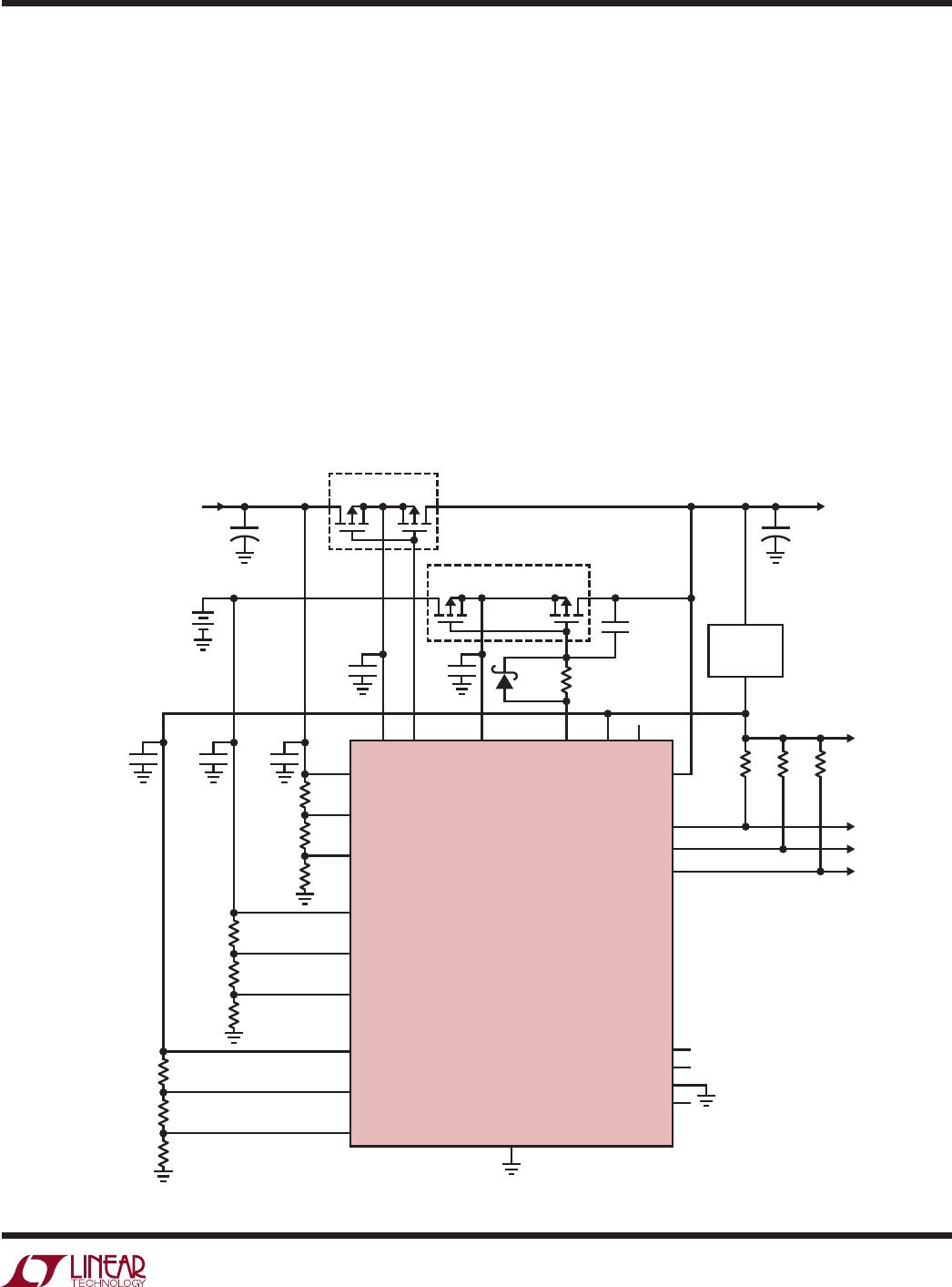
DESIGN EXAMPLE
A 2A multiple input supply system consisting of a 12V
supply with a source resistance of 20mΩ, 7.4V main
lithium-ion battery, and a backup 7.4V lithium-ion battery
is designed with priority sourcing from the 12V supply,
as shown in Figure 13. Power is sourced from the main
battery when the 12V supply is absent and the backup
battery is only used when the main battery and 12V supply
are not available. The ambient conditions of the system
will be between 25°C and 85°C.
The design limits the output voltage droop to 800mV
during switchover. The load capacitor is assumed to have
a minimum ESR of 50at 85°C and 80 at 25°C
through paralleling low ESR rated aluminum electrolytic
capacitors. The input source is allowed to drop 1V.
Selecting External P-Channel MOSFET
The design starts with selecting a suitable 2A rated
P-channel MOSFET with desired
R
DS(ON)
. Reviewing several
MOSFET options, the low 18R
DS(ON)
, dual P-channel
IRF7324 with a –20V BV
DSS
, is chosen for this application.
The low 18R
DS(ON)
results in a 72mV combined drop
at 25°C and 85mV drop at 85°C. Each P-channel MOSFET
dissipates 72mW at 25°C and 85mW at 85°C.
Inrush Current Limiting
When connecting a higher voltage source to a lower voltage
output, significant inrush current can occur. The magnitude
of the inrush current can be calculated with Equation (19).
I
INRUSH
=
V1 V
OUT(INIT)
R
SRC
+ESR(C
L
)+ 2 R
DS(ON)
(19)
where V
OUT(INIT)
is the V
OUT
voltage when initially powered
from a supply voltage less than V1, V1 is the higher voltage
source, R
SRC
is source resistance of V1, ESR(C
L
) is the
ESR of the load capacitor, and R
DS(ON)
is the on-resistance
of the external back-to-back MOSFET.
Given a total series resistance from input to output, the
worst case inrush current will occur when V1 is running
20% high, at 14.4V, and V
OUT
is at its undervoltage limit
of 5.6V. During this condition, a maximum inrush current
of 83A will occur, as shown in Equation (20).
I
INRUSH
=
14.4V 5.6V
20mΩ+ 50mΩ+36mΩ
= 83A
(20)
Because the 83A of inrush current exceeds the 71A ab-
solute maximum pulsed drain current rating, I
DM
, of the
IRF7324, inrush current limiting is required.
Calculating the load capacitance, C
L
, and inrush current
limiting circuitry component, R
S
, is an iterative process.
To start, use Equation (14), with 0.79 R
S
C
S
initially set
to 10µs. To limit the output voltage droop to the desired
800mV, reserve 200mV for initial droop due to the load
current flowing in the ESR of the output capacitor. Next,
choose C
L
to set the maximum V
OUT
droop to 600mV, as
shown in Equation (21).
C
L
=
2A (3µs+12µs+10µs)
600mV
C
L
= 83.3µF
(21)
For margin, choose the initial C
L
value equal to 100µF and
use Equation (16) to determine R
S
. With an allowable 1V
input voltage drop and source resistance, R
SRC
, of 20mΩ,
the input voltage droop of 700mV is used to set the inrush
current of 35A. The other terms in the equation come
from the external P-channel MOSFET manufacturer’s data
sheet. The transfer characteristics curve shows the gate
voltage, V
GS
, is approximately 1.8V when driving the 35A
inrush current and the capacitance verses drain-to-source
voltage curve shows the maximum C
RSS
is approximately
600pF. C
S
is set to be greater than ten times C
RSS
, or
6.8nF. To ensure the designed inrush current is lower
than the absolute maximum pulse drain current rating,
I
DM
, calculate R
S
using the maximum value forV
G(SINK)
and C
L
, and the minimum value for C
S
. For aluminum

LTC4417HUF#PBF

Mfr. #:
Manufacturer:
Analog Devices / Linear Technology
Description:
Power Management Specialized - PMIC 2.5V to 36V Prioritized Triple PowerPath Controller
Lifecycle:
New from this manufacturer.
Delivery:
DHL FedEx Ups TNT EMS
Payment:
T/T Paypal Visa MoneyGram Western Union