LTC2655
10
2655f
Note 1: Stresses beyond those listed under Absolute Maximum Ratings
may cause permanent damage to the device. Exposure to any Absolute
Maximum Rating condition for extended periods may affect device
reliability and lifetime.
Note 2: All voltages are with respect to GND.
Note 3: Linearity and monotonicity are defi ned from code k
L
to code 2
N
–1,
where N is the resolution and k
L
is the lower end code for which no output
limiting occurs. For V
REF
= 2.5V and N = 16, k
L
= 128 and linearity is
defi ned from code 128 to code 65535. For V
REF
= 2.5V and N = 12, k
L
=8
and linearity is defi ned from code 8 to code 4095.
Note 4: Inferred from measurement at code 128 (LTC2655-16), or code 8
(LTC2655-12).
Note 5: DC Crosstalk is measured with V
CC
= 5V and using internal
reference, with the measured DAC at mid-scale.
Note 6: This IC includes current limiting that is intended to protect the
device during momentary overload conditions. Junction temperature can
exceed the rated maximum during current limiting. Continuous operation
above the specifi ed maximum operating junction temperature may impair
device reliability.
Note 7: Temperature coeffi cient is calculated by dividing the maximum
change in output voltage by the specifi ed temperature range. Maximum
temperature coeffi cient is guaranteed for C-grade only.
Note 8: Digital inputs at 0V or V
CC
.
Note 9: Guaranteed by design and not production tested.
Note 10: Internal Reference mode. DAC is stepped 1/4 scale to 3/4 scale
and 3/4 scale to 1/4 scale. Load is 2k in parallel with 200pF to GND.
Note 11: V
CC
= 5V (-H Options) or V
CC
= 3V (-L Options), internal
reference mode. DAC is stepped ±1 LSB between half-scale and
half-scale – 1. Load is 2k n parallel with 200pF to GND.
Note 12: DAC to DAC Crosstalk is the glitch that appears at the output
of one DAC due to a full scale change at the output of another DAC. It is
measured with V
CC
= 5V and using internal reference, with the measured
DAC at mid-scale.
Note 13: C
B
= Capacitance of one bus line in pF.
Note 14: Gain error specifi cation may be degraded for reference input
voltages less than 1V. See Gain Error vs Reference Input Curve in the
Typical Performance Characteristics section.
ELECTRICAL CHARACTERISTICS
LTC2655
11
2655f
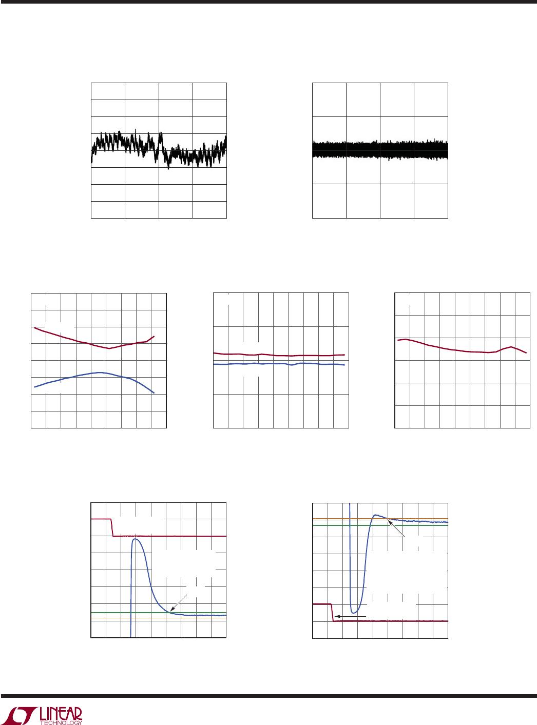
DNL vs Temperature
REFIN/OUT Output Voltage
vs Temperature
Settling to ±1LSB Rising
Settling to ±1LSB Falling
Integral Nonlinearity (INL) Differential Nonlinearity (DNL)
INL vs Temperature
CODE
128
INL (LSB)
4
3
–2
–3
–1
2
1
0
–4
32768 4915216384
2655 G01
65535
V
CC
= 3V
CODE
128
DNL (LSB)
1.0
–0.5
0.5
0
–1.0
32768 4915216384
2655 G02
65535
V
CC
= 3V
TEMPERATURE (°C)
–50
INL (LSB)
4
–2
2
3
1
–1
–3
0
–4
503010 1109070–10–30
2655 G03
130
V
CC
= 3V
INL(POS)
INL(NEG)
TEMPERATURE (°C)
–50
DNL (LSB)
1.0
–0.5
0.5
0
–1.0
503010 1109070–30 –10
2655 G04
130
V
CC
= 3V
DNL(POS)
DNL(NEG)
TEMPERATURE (°C)
–50
V
REF
(V)
1.253
1.248
1.249
1.252
1.251
1.250
1.247
503010 1109070–30 –10
2655 G05
130
V
CC
= 3V
2µs/DIV
V
OUT
250µV/DIV
SCL
3V/DIV
2655 G06
9TH CLOCK OF
3RD DATA BYTE
7.8µs
1/4 SCALE TO
3/4 SCALE STEP
V
CC
= 3V, V
FS
= 2.50V
2µs/DIV
V
OUT
200µV/DIV
SCL
3V/DIV
2655 G07
9TH CLOCK OF
3RD DATA BYTE
7.3µs
3/4 SCALE TO
1/4 SCALE STEP
V
CC
= 3V, V
FS
= 2.50V
R
L
= 2k, C
L
= 200pF
AVERAGE OF 2048 EVENTS
TYPICAL PERFORMANCE CHARACTERISTICS
T
A
= 25°C unless otherwise noted.
LTC2655-L16
LTC2655
12
2655f
TYPICAL PERFORMANCE CHARACTERISTICS
T
A
= 25°C unless otherwise noted.
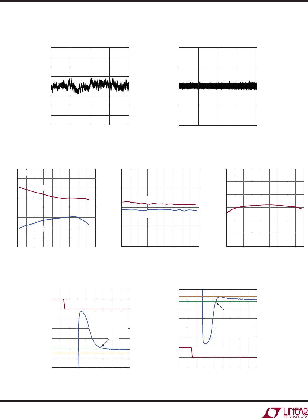
LTC2655-H16
Integral Nonlinearity (INL) Differential Nonlinearity (DNL)
CODE
128
INL (LSB)
4
–2
–1
–3
2
3
1
0
–4
32768 4915216384
2655 G08
65535
V
CC
= 5V
CODE
128
DNL (LSB)
1.0
–0.5
0.5
0
–1.0
32768 4915216384
2655 G09
65535
V
CC
= 5V
Settling to ±1LSB Rising Settling to ±1LSB Falling
2µs/DIV
V
OUT
250µV/DIV
SCL
5V/DIV
2655 G13
9TH CLOCK OF
3RD DATA BYTE
7.9µs
1/4 SCALE TO
3/4 SCALE STEP
V
CC
= 5V, V
FS
= 4.096V
R
L
= 2k, C
L
= 200pF
2µs/DIV
V
OUT
250µV/DIV
SCL
5V/DIV
2655 G14
9TH CLOCK OF
3RD DATA BYTE
5.5µs
3/4 SCALE TO
1/4 SCALE STEP
V
CC
= 5V, V
FS
= 4.096V
R
L
= 2k, C
L
= 200pF
INL vs Temperature DNL vs Temperature
Reference Output Voltage
vs Temperature
TEMPERATURE (°C)
–50
INL (LSB)
4
–2
2
3
1
–1
–3
0
–4
503010 1109070–10–30
2655 G10
130
V
CC
= 3V
INL(POS)
INL(NEG)
TEMPERATURE (°C)
–50
DNL (LSB)
1.0
–0.5
0.5
0
–1.0
503010 1109070–30 –10
2655 G11
130
V
CC
= 3V
DNL(POS)
DNL(NEG)
TEMPERATURE (°C)
–50
V
REF
(V)
2.054
2.044
2.046
2.052
2.050
2.048
2.042
503010 1109070–30 –10
2655 G12
130
V
CC
= 5V

LTC2655IUF-H12#TRPBF

Mfr. #:
Manufacturer:
Analog Devices Inc.
Description:
Digital to Analog Converters - DAC 12-Bit I2C Quad DAC (2.048V Reference)
Lifecycle:
New from this manufacturer.
Delivery:
DHL FedEx Ups TNT EMS
Payment:
T/T Paypal Visa MoneyGram Western Union