LTC2655
16
2655f
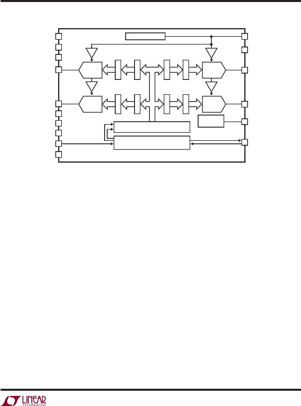
PIN FUNCTIONS
REFLO (Pin 1/Pin 20): Reference Low. The voltage at this
pin sets the zero-scale voltage of all DACs. This pin should
be tied to GND.
V
OUTA
to V
OUTD
(Pins 2,4,13,14/Pins 1, 3, 13, 14): DAC
Analog Voltage Outputs. The output range is 0V to 2 times
the voltage at the REFIN/OUT pin.
REFCOMP (Pin 3/Pin 2): Internal Reference Compensation.
For low noise and reference stability, tie 0.1µF capacitor
to GND. Connect to GND to use an external reference at
start-up. Command 0111b must still be issued to turn off
internal reference.
REFIN/OUT (Pin 5/Pin 4): This pin acts as the internal
reference output in internal reference mode and acts as
the reference input pin in external reference mode. When
acting as an output the nominal voltage at this pin is
1.25V for -L options and 2.048V for -H options. For low
noise and reference stability tie a capacitor from this pin
to GND. Capacitor value must be ≤ C
REFCOMP
. In external
reference mode, the allowable reference input voltage
range is 0.5V to V
CC
/2.
LDAC (Pin 6/Pin 5): Asynchronous DAC Update. A fall-
ing edge on this input after four bytes have been written
into the part, immediately updates the DAC register with
the contents of the input register. A low on this input
without a complete 32-bit (four bytes including the slave
address) data write transfer to the part does not update
the DAC output. Software power-down is disabled when
LDAC is low.
CA2 (Pin 7/Pin 6): Chip Address Bit 2. Tie this pin to V
CC
,
GND or leave it fl oating to select an I
2
C slave address for
the part (Table 2).
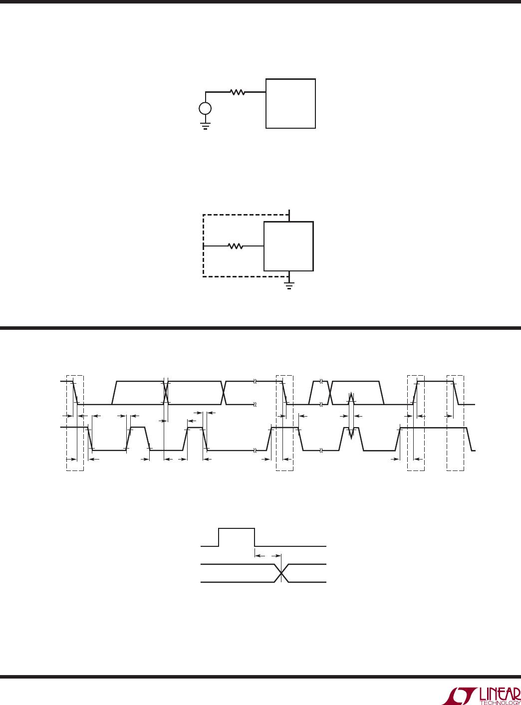
SCL (Pin 8/Pin 7): Serial Clock Input. Data is shifted
into the SDA pin at the rising edges of the clock. This
high impedance pin requires a pull-up resistor or current
source to V
CC
.
SDA (Pin 9/Pin 9): Serial Data Bidirectional. Data is shifted
into the SDA pin and acknowledged by the SDA pin. This is
a high impedance pin while data is shifted in. It is an open-
drain N-channel output during acknowledgement. This pin
requires a pull-up resistor or current source to V
CC
.
CA1 (Pin 10/Pin 10): Chip Address Bit 1. Tie this pin to
V
CC
, GND or leave it fl oating to select an I
2
C slave address
for the part (Table 2).
CA0 (Pin 11/Pin 11): Chip Address Bit 0. Tie this pin to
V
CC
, GND or leave it fl oating to select an I
2
C slave address
for the part (Table 2).
PORSEL (Pin 12/Pin 12): Power-On-Reset Select. If tied
to GND, the part resets to zero-scale at power-up, if tied
to V
CC
, the part resets to mid-scale.
V
CC
(Pin 15/Pin 18): Supply Voltage Input. For -L options,
2.7V ≤ V
CC
≤ 5.5V, and for -H options, 4.5V ≤ V
CC
≤ 5.5V.
Bypass to ground with a 0.1µF capacitor placed as close
to pin as possible.
GND (Pin 16/Pin 19, Exposed Pad Pin 21): Ground. Must
be soldered to PCB Ground.
DNC (NA/Pins 8, 15, 16, 17): Do not connect these
pins.
(GN/UF)